The copper thickness in the printed circuit boards (PCBs) is a decisive element that influences the functionality, performance, and lifetime of the final product.
In this guide, we will explore copper thickness, how it is a component that can affect PCB designs, why it is important to use standards and all the things you need to consider when choosing copper thickness for various applications.
What is PCB Copper?

PCB has copper as its primary component and it actually is the thin layer of copper foil that is directly placed on the base of the electronic board. It serves as a primary lead for electronic signal and electricity via switchboards. PCB copper is a vital element in the creation of conductive tracks, padding and vias, that are components which are used to join the various segments of the printed circuit board. Thus, they create the pathways that become the circuits found on the PCB. These copper tracks are usually etched in order to accomplish the right circuit design during the fabrication of the circuit. The copper tracks of a PCB (Board) bear a truly indispensable role in making equipment and electronics function as intended and in delivering dependability and high performance.
Types of Copper Used in PCBs
Two main types of copper are commonly used in PCB manufacturing:
Electrolytic (ED) Copper

- Copper foils have to sink production, which is a high-purity copper foil that is treated by electroplating.
- It is generally an inner layer for the PCB, which makes a flat and smooth surface area.
- ED copper is recognized for its top-notch electrical conductivity and it becomes a perfect instance where the space and line thickness restrictions apply.
- It finds its application in multi-layered PCBs, where signal integrity becomes a decisive factor and impedance concerns are realized.
Rolled Annealed (RA) Copper

- One of the principal processes responsible for enhancing the material properties of Copper is rolling and annealing, which contribute to the end result.
- In this process, RA copper is more suitable for layers located near the surface of the PCB since it has better chemical processibility and groove roughness.
- It plays an important role in providing good bonding for solder masks and component adhesive during the process of PCB assembly.
- The application of lead-free level RA copper is important in single- or double-faced PCBs where the conductive quality, flatness, and suitability for soldering are critical.
How are copper weight and thickness measured on a PCB?
Copper weight and board thickness are typically measured using various methods, including:
Copper weight measurement:
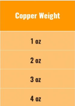
- Copper weight on PCB is generally referred to as ounces per square inch (oz/ft2) or grams per square meter (g/m2).
- The most commonly used method for measuring copper weighs is based on weighing a selected area of copper film (foil) on a high-accuracy or precision scale with one’s available or ready access.
- On the other hand, copper weight may be assessed either by calculating the thickness of the copper foil and its area or by some other method.
Copper Thickness Measurement:
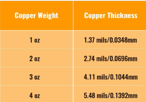
- Thickness of copper (PCBs) is normally measured in mils, with one mil = 0.001 inches or in micrometers (µM).
- Various techniques can be used to measure thickness of the copper evenly, including:
- Eddy Current Testing: This highly sensitive method uses eddy currents, which are induced electric currents, to measure copper and other conductive materials.
- X-ray Fluorescence (XRF) Analysis: The method of X-Ray Fluorescence (XRF) can be used to determine the thickness of copper layers by detecting either the characteristic X-ray emissions coming from the material or the attenuation of the X-rays.
- Microsectioning: With this destructive test method, the PCB is also cut in a cross-section, and then its copper layer thickness is measured by using a microscope for the measurement.
Application of Copper in PCBs
The application of copper in PCBs involves several steps in the manufacturing process:
- Preparation of Substrate:
- Generally, the process starts with a substrate material like FR-4 (fiberglass-reinforced epoxy resin) or another corresponding dielectric material.
- The substrate is cleaned, and the adhesion for the copper foil is prepared.
- Copper Foil Preparation:
- Copper foil, whose thickness and quality are to be depended upon, is picked most frequently in folded form as rolls.
- The copper adhesion may be prepared with treatment of the surface, such as cleaning, surface roughening, and/or applying adhesion-promoting coatings to promote bonding with the substrate.
- Lamination:
- During the lamination process, copper-clad laminate that has been prepared is glued to the substrate material.
- This is usually achieved using a lamination press that combines heat and pressure to attach the copper-clad laminate to the substrate.
- Copper Clad Laminate is bonded to the substrate by heat, pressure, and tackiness in such a way that all elements work together to create a strong bond.
- Etching:
- Once laminated, the copper foil is covered with a layer of photoresist, which is a light-sensitive material.
- An analog process, which is based on the same principle as the image transfer process, is used to put the circuit pattern on the photoresist layer.
- The copper layer is then dipped into the chemical solution, which will etch away the copper only in the exposed areas, thus creating the circuit traces and the pads.
- Strip and clean:
- Once the etching process has finished, the rest of the resists are removed, and the copper traces are cleaned.
- The PCB could be further washed to undertake cleaning processes aiming at removing the etching process’s residues.
- Surface Finish (optional):
- The zinc and copper will be exposed in the areas required by application. This may lead to corrosion and oxidation. Based on the application requirements, the exposed surfaces may undergo surface finish treatments such as plating of Gold, Tin, or other metals to enhance solderability and protect against corrosion.
- Inspection and Testing:
- The inspected PCB goes through various electrical inspections and testing to ensure that the copper traces, pads, and other copper features are properly positioned with good contact and size as designed and indicated on the layout.
- This could be a combination of the visual inspection, electrical testing and other quality assurance functions.
How to Select PCB Copper Foil Thickness?
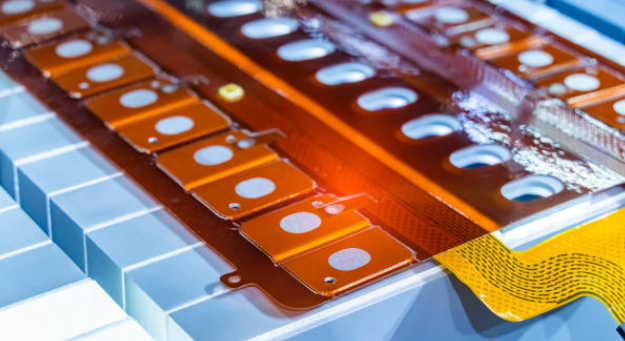
Choosing the right copper foil thickness for the printed circuit board is a major concern for its electrical performance, thermal management, and manufacturability. Here are some steps to guide you in selecting the right copper foil thickness for your PCB design:
- Consider Electrical Requirements:
- Know the maximum electrical capacity of your PCB, such as the amount of current which your designed circuit can carry, impedance control, and the necessity for signal integrity.
- Thin copper foils involve little power being lost as heat while higher currents can easily pass through. In case of design which has high current pathways, a copper sheet of bulkier power may be needed.
- Evaluate Thermal Considerations:
- Analyze the thermal management requirements of your PCB, taking into account the factors including the power dissipation, thermal conductivity and the available heat sinking.
- Thick copper foils can provide better thermal conductivity and heat dissipation performance. When talking about the heat transport ability, thicker copper foils may come handy in high-performance devices.
- Review Manufacturing Constraints:
- Consider the manufacturing abilities and limitations of your PCB fabrication technique.
- Thicker copper foils should be taken into account during etching, drilling and plating processes, involving appropriate techniques of adjustment. Verify your copper sheet thickness with the manufacturer to make sure your pick is up to their options.
- Balance Cost Considerations:
- Analyze the implications on the costs by giving the different copper sheet thickness as the options.
- Copper foils with higher bulkiness will therefore be more expensive and usually require extra vinyl layers or silver which increase the manufacturing costs.
- Consult Design Guidelines and Standards:
- Regarding copper foil thickness, generate guideline recommendations that are based on the PCB industry standards and are appropriate for different application and design aspects.
- Standard organization may issue such thin support skins bulkier standards with respect to the functionality taking into consideration current carrying capacity and signal integrity, among other factors.
- Perform Simulation and Analysis:
- Employ simulating tools and analysis software to analyze the efficiency of your PCB design parallel to that of copper foil, which has several excessive thicknesses.
- Use simulations to determine impedance control issues, signal integrity factors, thermal dissipation, and ensure manufacturability to achieve optimum design.
- Iterate and Optimize:
- Modify the PCB designed several times, considering different copper foil thickness and performing the performance, cost, and manufacturability analyses each time.
- The design must be optimized according to the results of simulating, analyzing, and practical issues to get the best electrical performance, thermal management, and expenditure.
Does using Thicker Copper Provide Efficient Performance to PCBs?

Copper becoming more copper and thicker heavy copper used naturally in PCBs does provide more efficiency to some conditions. Here’s how:
- Improved Current Handling: Copper layers that are more thick get lower resistance in crawling the higher amps down efficiently. This is especially important in high-voltage applications where minimizing Zo loss is necessary for decreasing resistive losses and efficiency is critical.
- Enhanced Thermal Management: Bulkier copper layers provide for better thermal conductivity, which enables these components to get rid of heat very efficiently. This would avoid inner components from being overheated, thus ensuring longer-term reliability and good efficiency of the system through this process.
- Reduced Voltage Drop: Bulkier copper layers produce lower resistance values, hence the power loss, which is relatively considered to be rapid. It is required to maintain predictable voltage levels and signal integrity, especially in circuits with considerable time traces or high-frequency signals. Maintaining the correct voltage level minimizes the occurrence of low voltage, thus improving the operation of the circuit. Hence, minimizing voltage drop contributes to the efficient operation of the circuit.
- Better Signal Integrity: Copper foils with thicker layers can be used in order to keep signal quality unaffected by lowering reflection, distortion and losses. This is particularly important to use in places with a large volume of digital and RF signals, where data quality plays a vital role in the efficient transfer of information.
- Mechanical Durability: The higher percentage of copper layers increases the PCB’s mechanical strength to a certain point, which leads to enhanced durability and resistance to mechanical stresses. This will result in a harvesting of the reliability and durability of the PCB, bringing about significantly more efficient system.
General Guidelines for Minimum Spacing by Copper Weight
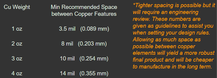
PCB design and production process guidelines for spacing copper weight in general can be different based on specific PCB design, manufacturing process and industry standards. However, here are some approximate guidelines for copper weights that are commonly followed:
- For Internal Traces (Signal Layers):
- For inner layers of the PCB, where traces are insulated by the substrate material:
- With copper (35 µm) thickness, min spacing of 0.006″–0.008″ is general for wiring, which is around 0.15 mm-0.20 mm.
- The smallest clearance between the stationery and the incising will be from 0.008 inches (0.20 mm) to 0.010 inches (0.25 mm) on the least pattern.
- Spacing may be larger than that if the copper plating is 3 oz or more and typically with a minimum of 0.010 inch or 0.25 mm.
- For inner layers of the PCB, where traces are insulated by the substrate material:
- For External Traces (Outer Layers):
- For traces exposed on the outer layers of the PCB, where solder mask and silkscreen are applied:
- For 1 oz copper, the size range of 0.005 inches (0.127 mm) or 0.006 inches (0.15 mm) is commonly given.
- With 2 oz copper, spacing’s min might be as much as 0.006 inches (0.15 mm) to 0.008 inches (0.20 mm).
- In the case of a tolerant surface and 3 oz or higher copper, minimum spaces may get wider, likely beyond 0.20 mm (0.008 inches).
- For traces exposed on the outer layers of the PCB, where solder mask and silkscreen are applied:
Conclusion
In summary, PCB copper serves pivotal functions in terms of reliability, usability, and power of printed circuit boards (PCBs). With copper being responsible for the transfer of electrical signals and power distribution, selecting the required copper thickness and weight is significant to creating a suitable design as well as removing the risk of malfunction. Thicker copper conductors have several benefits, such as improved heat dissipation, enhanced power transference, and stronger signal transmission. Yet, thoughtful consideration of issues like electricity demand, thermal constraints, manufacturability issues, and price shape would finally help to choose an optimum level of copper thickness for each PCB design. Through correlation with PCB manufacturers’ guidelines, a design engineer can focus on different PCB copper capabilities, such as copper features such as dissipation factor and current layer, to design a reliable electronic system.
Frequently Asked Questions
Here are some FAQs about PCB copper thickness:

