PCB is just one of the components in the manufacturing process, and it is affected by the copper thickness utilized by designers. The thickness directly affects the electrical performance, thermal management, and mechanical strength of the final product. A copper’s thickness issue matters whether you’re a hobbyist, an engineer, or own a PCB manufacturing company, as it is one of the factors to be considered when making wise design decisions.
This blog article deals with the problem of why thickness is of great significance, as well as how it can be measured and what thoughts should be kept in mind when making a choice.
What is copper weight/copper thickness?
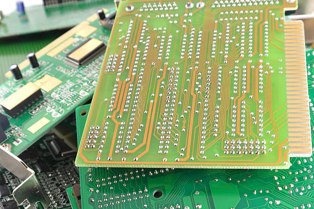
Copper weight, that is, the thickness of copper on a printed circuit board (PCB), plays an instrumental role in the electrical characteristics of the circuit, which range 1 oz to 3 oz. It is commonly reported either in ounces per square foot (oz/ft2) or in units related to micrometers (µm). Basically, it is the representation of the copper plating thickness on the circuit board during the manufacturing procedure, especially in copper foil.
Why thicker copper matter?
Copper thickness on a printed circuit board (PCB) matters for several reasons:
- Electrical Conductivity: The thickness of the copper on the PCB determines to what extent the traces will be able to tolerate the current without being overheated and how low the resistance will be across the line. The thickness of copper may be the determinant factor between lower resistance and more intense currents, which is both a power supply and a heat sink inhibitor.
- Thermal Management: Copper’s very high thermal conductivity helps it dissipate heat much faster than other materials by incorporating thicker copper layers. This, most of all, is relevant in structural designs that give rise to excessive heating of the parts.
- Mechanical Strength: Thick copper in a PCB with greater thicknesses can strengthen its structure, which in turn would prevent it from breaking down under physical stress and pressure. This may be critical when it refers to a board worn down by mechanical action or one used in extreme environments.
How Copper Thickness is Measured
The copper thickness of PCBs is usually oxcel. This measurement indicates how much copper is present on the surface and directly influences the board’s capabilities for finished copper thickness.
- The converted thickness is 1.37 millimeters, or 34.79 microns, and is equal to about 1 ounce per linear foot (1 oz/ft2).
- 2 oz/ft2 doubles the thickness; thicker wires can contain more current and disperse heat better.
Deciding on thickness is mainly based on the specific electrical performance requirements of your project, either in your inner layers or outer layers, taking into consideration both the cost and electric properties and required copper thickness.
How thick is a copper PCB?
As for the thickness of copper on a printed circuit board (PCB), the thickness may be written as ounces per square foot (oz/ft2), which could be converted into other linear measurements such as inches, which is common and familiar. Here’s how thick 1 oz, 2 oz, and 3 oz copper layers typically are:
- 1 oz of copper has a thickness of 1.37 mils, which is around 34,79 microns.
- 2 oz. of copper would be 2.74 mils, or 69.58 microns, in thickness.
- 3 oz. of copper stock is equal to 4.11 mils, or 104.37 microns.
These measurements represent the physical fact of the copper layer thickness determining the PCB’s ability to carry the current, the ability to dissipate the heat, as well as the overall mechanical robustness that is required for the for the copper thickness.
Copper Weight Minimum Spacing Rules
In PBC design, the copper foil channels determine the minimum segregation rules in terms of elements such as traces and pads. The protection of regulations helps to prevent electrical issues such as short circuits and electromagnetic interference that may affect the functioning and safety of a device. Here’s how copper weight impacts these spacing requirements:
- 1 oz. Copper: Minimum Spacing: As usual, the maximum flying distance for 1 oz of copper features is about 4 mils (0.004 inches). This can be applied in general-purpose cases where the amount of voltage and current is reasonably low.
- 2 oz. Copper: Minimum Spacing: thick Copper pcb commonly dictates the spacing to be considerably more generous at approximately 6 mil. or 0.006 inches and above. For this reason, a thicker copper layer is needed in order to push through more currents. The spacing between them should be kept greater to prevent heat accumulation and a short in the current.
- 3 oz. Copper: Minimum Spacing: The net copper is 3 oz, which means you might have to be prepared for the spacing even up to 8 mils (0.008 inches) of extension. Thus, there are both electrical and thermal considerations that are extended in cases of such size.
Why Would You Use Heavy Copper in a PCB?
Copper, mainly used in the landscape elements of PCB copper thickness, provides some purposes, such as applications with high power consumption, enhanced durability, copper-clad laminate, and temperature regulation. Here are the main reasons, presented as an ordered list:
- Increased Current Carrying Capacity: It is common to find that bulky copper cables can send much more current than slender copper feature cables, which is crucial for high-power electronics, for example, power supply units, automotive components, and others.
- Enhanced Thermal Management: Copper evenly with a greater thickness will be better at dissipating heat, and it might decrease the requirement for extra cooling mechanisms, which is extremely vital to the construction of small-sized electronic devices.
- Improved Mechanical Strength: PCBs with abundant copper are more rigid, so they can withstand either physical stress or vibration, which makes this type of PCB utilized for industrial & military purposes.
- Higher Endurance to Thermal Strains: The strongest copper foils PCBs have a superior ability to withstand temperature amplitude variations, making them most suitable for applications that experience frequent thermal fluctuations.
- Reduced Layer Count in Multilayer Boards: The current quantum per unit area that one can achieve is higher with the heavier copper-printed circuit boards, so the number of layers can be minimized in multilayer printed circuit boards, which simplifies the design process and may, therefore, reduce production costs.
- Integration of High-Power and Control Circuitry: Perhaps the main characteristic of multilayer circuit boards is the possibility to bring together the discrete wires that are used for the power circuits and control circuits into the same board, taking into account that this can lead to a significant reduction in the system size.
- Longevity and Reliability: Heavy copper PCBs are the best choice of the devices requiring survival operation as long as high temperatures and mechanical stress could cause the failure of their low-grade non-copper counterparts.
Choosing the Right Copper Thickness
In choosing the right copper thickness for your design, follow these rules:
- Assess your current requirements: Evaluate the current that each trace can accommodate, and trace copper thickness calculators found on the Web may be used to determine the required thickness for the properly designed PCB.
- Consider Thermal Needs: Should you have an application that generates a higher amount of heat, then thicker copper might be a better choice due to extensive heat dissipation.
- Understand Your Environmental Conditions: For instance, the higher class relays risk from harsh environments (vibration, handling) as much as the Ha further hefty copper may play an added substance.
- Budget Constraints: Higher copper thicknesses always lead to higher prices. Analyze if the rise in expenses is worth it. Evaluate them from the standpoint of reliability and performance.
Conclusion
Copper-thickness means more than just a technical parameter; it is an important design decision with a strong influence on the performance and lifetime of your printed circuit board. The copper thickness selection you make is a vital aspect of the optimal performance of your circuit boards; you should comprehend the matters at hand and select the copper that will give the best results for the application you intend.
The knowledge that comes as a result of this enterprise about copper thickness will be the tool that you need to make correct decisions on the basis of PCB designs. Think, in terms of thickness, is one that excellently addresses your application’s want, exactly on the budget you can afford to direct to the project.