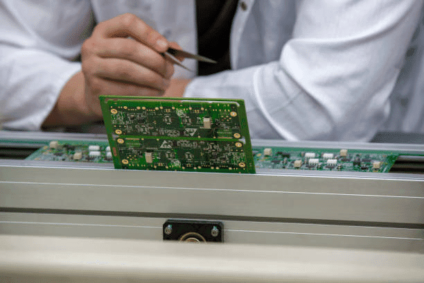
Mastering PCBA: The Essential Guide to Printed Circuit Board Assembly
Printed Circuit Board Assembly (PCBA) is a crucial process in the manufacturing of electronic devices, encompassing the soldering of various electronic components onto a printed circuit board (PCB). This assembly transforms a PCB into a fully functional electronic circuit integral to everything from consumer electronics to industrial machinery. The blog post explores different PCBA techniques, notably Surface Mount Technology (SMT) and Through-Hole Technology (THT), detailing their applications, benefits, and suitability for various types of electronic components. It emphasizes the importance of understanding both PCB and PCBA to achieve efficient manufacturing outcomes necessary electronic components, and highlights best practices and challenges in the PCBA process, aiming to provide a comprehensive guide to mastering PCBA for reliable and effective electronic device production.
Mastering HDI PCB Design: Techniques and Trends for High-Density Interconnects
The document titled “Mastering HDI PCB Design: “Seminar: High-Density Interconnects (HDI)/PCB Technology” delivers an in-depth investigation of high-density interconnect (HDI) PCB technology, which is vital to the creation of next-generation miniaturized electronic products with higher speed and lower power consumption. It describes the key characteristics of HDI, like microvias, which are very tiny lines with fine spaces, and advanced materials that infiltrate the signals and provide heat management to high density interconnection layers to the incorporate hdi boards. The paper concentrates on particular design methods, such as using high-end photolithography for perfect pattern formation and smart layer patterns to ensure increased conduction and higher wiring density. It covers HDI PCB layout materials, including commonly used ones like FR-4, polyimide, and PTFE, each having specific benefits used in particular applications to cpu and gpu chips with layer pairs also application of portable video recording devices. Besides that, the specific manufacturing requirements are also emphasized with the intricate manufacturing demands for HDI PCBs, meaning that the utmost care needs to be employed in order to be able to squeeze in a compact and complex circuit layout. This guide will be very useful to professionals in the design industry seeking to incorporate HDI technology into their electronic projects.
Unlocking the Potential: A Comprehensive Guide to Blank PCB Board
The document “Unlocking the Potential: This is how we introduce the subject of PCBs as a fundamental component of the process of electronic design and manufacturing and “Blank PCB Board” is this final article. By playing the role of the unoccupied “PCB” board as a plant board, the primary purpose of this breadboard provides us to comprehend the practical implications and the details of the PCB technology into action by implementing electronic components and conductive path. The topic will be presented from the variety of DBA bare PCBs, including single-sided, double-sided, multilayer, flexible and rigid-flex PCBs among others. This explaining shall involve unwrapping the uses of the technologies and the techxitventions and how they are taking the skateboard industry to new heights. Moreover, it outlines the central materials used for PCB manufacturing like FR-4 and metal cores, highlighting how the latter wood strongly affect the (board’s) performance during its production. That guide is also responsible of the importance of proper processing, dryer chemical application and choosing high quality woods i order to reach a better lumber yield. As for methodologies of testing, a detailed clarification of trade-offs between different approaches for the preparation of assembly stage with a particular focus on the quality assurance procedures will also be discussed. In essence, the article is a thorough guide concentrating on main aspects of manufacturing blanked PCBs that remain relevant in electronic making.
Unveiling PCB Surface Finish Types: A Comprehensive Guide to Choosing the Right One
The document titled “Unveiling PCB Surface Finish Types: This article “The Guide to The Right One for the Protected Printed Circuit Boards” gives a detailed review of the DC surface finish options which are pertinent to the PCBs that protect from corrosion and ensures that the components are soldered reliably. In it, the coverage of the different finishes such as Hot Air Solder Leveling (HASL), Lead-Free HASL, Electroless Nickel Immersion Gold (ENIG) as well other finishes are discussion, their advantages, disadvantages, and suitability to various applications.The thread references cost, environmental effect, and whether the surface texture is compatible for certain pieces or not. This helps the manufacturer and the designer to make well-informed decisions for effective PCB performance.
Mastering Flex PCB Design: Essential Tips and Techniques for Innovative Circuitry
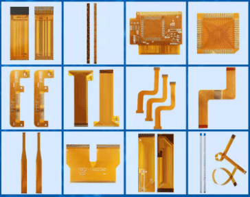
The document titled “Mastering Flex PCB Design: In this paper, “Flex Cuircatter Innovation: Essential Hints and Techniques for Flexible Printed Circuit Boards” delves in to depth of flexible printed circuit boards’ soaring use in the modern electronics and gives the reasons of their increasing attention: Flex PCBs due to their flexibility and high functionality. The chapter begins with Flex PCB characteristics and them outlines various types of this technology involving single-sided, double-sided, multilayer, rigid-flex, and sculptured flex circuits. The article explains the benefits of the Flex PCBs, which include the saving in space, having a lightweight design, strong reliability, and a great flexibility. In this section, the article also covers about the materials used in Flex PCBs, for example polyimide and copper, and discusses aspects that need to be considered in the design if you are expecting the Flex PCB projects to be successful. Additionally, the article give the address of the most frequent issues and solutions for Flex PCB designing and manufacturing, which detail step by step instructions for designing circuits effectively. The complete coverage, including all the capabilities that it has, will provide the designers with skills to innovate and bring forth new applications of Flex PCB that are suitable for various electronic products.
Vital Connections: Unveiling the Role and Types of Vias PCB Design
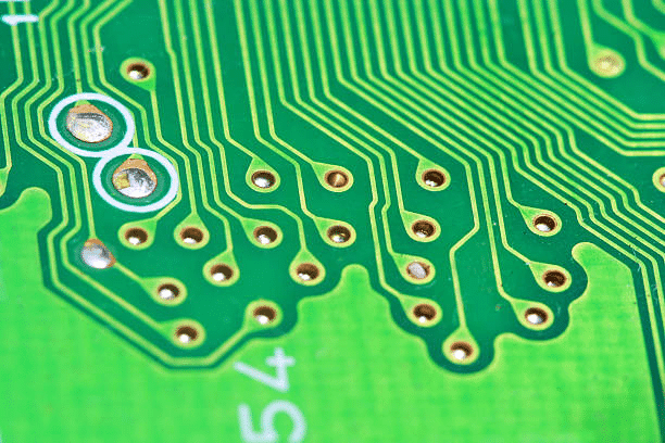
The essence of good design and routing with PCB vias lays the foundation to the highest quality circuit boards with reliability and performance as the main focus. Initiate this process by getting first-hand information about your board that will include the electric, thermal, and mechanical requirements among others. Analyze your design features as well as the PCB design under the matrix theory, and use the via types, which include through-hole, blind, buried or microvias, accordingly into the conductive tube. Pay meticulous attention to your vias stack sequence during outer layer and inner layer planning in order to successfully accommodate them and ensure a good signal route. Deciding on the ideal sizes of your vias and their shape in a way that both takes current capacity and manufacture into consideration. Apply as much as possible low number of via in the signal pathers, and design the thermal vias below the energy heaters positioned for the venting of unusable heat. Ensure you keep communications with your PCB supplier open and discuss the general nature of your project with regard to their manufacturing facilities. Use dedicated software for PCB design, as it is available, to check and avoid errors. Additionally, make the fabrication process a detailed one that involves you in at every phase of the process. This will ensure you are contented with the fabrication. These components carry a string of functions, which integrates and improves the reliability of the PCB.
Understanding Copper Thickness PCB: What You Need to Know
Copper weighs a lot, which is a major asset for those PCBs that are required to function properly when there is a high power input for the best thermal management and also for long-term durability that resulting thickness. Copper should be recommended for use, as it can carry a larger current since it has a high current-carrying capacity. Also, Cu has superior thermal conductivity, which helps with heat generation in power-intensive appliances and prevents supplementary cooling devices. Furthermore, the structural durability brought about by these heavy copper PCBs makes them perfectly fit in environments that may experience different stresses and strains, such as temperature ones with the desired thickness of pcb fabrication to the internal layers or external layers. This metal’s combination of properties gives it a high position when it comes to the number of lines in multilayer circuits, the integration of high power and control schemes on one board, and reliability and longevity in critical implementations.
Demystifying PCBs: Understanding Standard pcb Thicknesses for Optimal Performance
The production of printed circuit board thickness (I-CB) is perhaps an understated but yet more critical process in the world of electronics. An instance of minute information that features prominently in how PCBs perform is the thickness they come in. This article considers the importance of grasping the standard PCB thickness reduction and gives electronic engineers the opportunity to improve the performance of their products. It explains how the PCB thickness affects structural integrity, signal quality, and heat dissipation, showing its influence on such aspects as the cost of production and reliability of the final product. The most traded samples exist as 1.6mm, but it is done in depth to show how these standard thicknesses are vital for different applications and hence how typical PCBs function as well as their compatibility. In such way, the article draws the curtain on weighing factors behind single-layer PCB and multilayer PCB and provides a guide to designers and engineers so that they can get the optimum thickness of PCBs for their applications.
Decoding 1 oz Copper Thickness: What It Means for Your PCB Performance
This 1 oz per square foot thickness copper offers true performance as well as the economy and utility of the PCB board during the final application. The film thickness is 1.4 mils (35.55 μm), which is widely used in all industries because it can moderately treat the current in a load while providing effective heat dissipation and mechanical strength too. The copper 1 oz. is great to use on any consumer electronics, on the automotive system, and for many general applications. It is a cost-effective way to solve many different needs in a simple way, which is why you find so many designers making use of it.
Decoding the Circuit: An Expert Guide to PCB Reverse Engineering
PCB reverse engineering stands for opening a board and then studying its design, features, and functionality, without original blueprints in most cases. This process is beneficial to mankind for documentary making, improvement, competition monitoring, security examination, economic reduction, and educational purposes. A structured approach involving state-of-the-art tools and technologies is needed while addressing issues such as organ complexity, angioarchitecture form, and unknown components. In this regard, the procedure is regulated by intricate legal and ethical coercion to protect copyright ownership. In brief, PCB reverse engineering becomes a significant practice that improves our domain knowledge throughout the process of future electronics development.