Striking the Right Balance: Navigating PCB Thickness Standards for Enhanced Electronics Performance
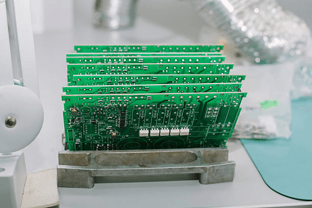
Thickness of a printed circuit board or PCB is an indispensable measure that determines several properties of this element, including its mechanical stability, thermal properties and usefulness. Traditional and common thicknesses of PCBs under consideration include 1. 6 mm, 1. 2 mm, and 0. have thickness of 8 mm and can be selected according to characteristics of the loading application and type. Highercopper wires are better when it comes to mechanical reinforcement and thermal dissipation to ensure that the PCBs are fit for application that require high voltage and heat. On the other hand, miniaturized PCBs are preferred if you are concerned about the size and weight of your device. Determining the right PCB thickness means understanding several factors such as the stack height, the electrical characteristics, heat flow, fabrication techniques, and common practices in the circuit manufacturing sector.
Diving into the Heart of PCBs: Exploring PCB Core vs. Prepreg Materials
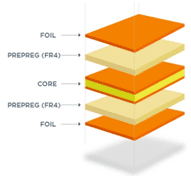
Thus, the core and prepreg materials are incredibly important to guarantee the working process of the final PCB product. Sometimes, the core is also available in other materials such as FR-4, metal, or polyimide for support structure, electrical insulation, and heat dissipation. Fiberglass prepreg is used for the bonding layer and for layers of insulation and heat sinks which are made from the same material. It is essential to understand these materials’ differences to materialize dependable and high-functionality PCBs since these differences affect the mechanical and electrical performances and overall resilience of the board.
The Ultimate Guide: We need to know that Why Circuit Boards are green.
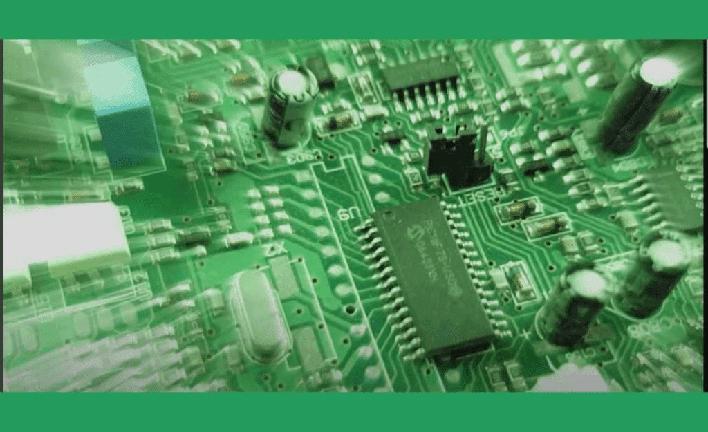
The arrays have a green color that is attributed to the green solder masks plated on the boards to cover the copper circuits. It is significant to note that this color choice can be attributed to their historical status as a manufacturing color, military-specified color, and other functional purposes. Green solder masks can be visually and superficially distinguished from the copper pads and lines as well as from the defects, which are easier to identify during the inspections carried out by both humans and optical instruments. They also withstand heat and offer firmness whenever the soldering process is to be under way. In furtherance of this argument, Cost is relatively low in the manufacturing of green and the color has earned its way into the standard due to standardization that will dictate consistency across products and projects.
A Comprehensive Guide to Cleaning Circuit Boards
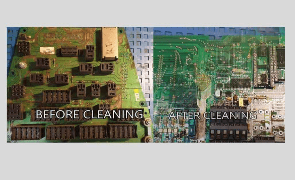
Circuit board cleaning is critical since it facilitates the functions of technology-based products and ensures they last long. Cooling is important so that contamination build up with dust, dirt or any other particle, so as to result in tolerance issues, electrical shorting or even failures. This cleaning process requires several tools that include the isopypol alcohol, much removers, ultrasonic cleaners and the soft bristle brushes. However, since they are fragile and are moved using a vacuum, special safety measures should be taken such as powering them off before handling them. The corrosion of the material can be avoided and the fabrication sustain the optimal functionality and durability in performing its duty by following several maintenance and cleaning procedures.
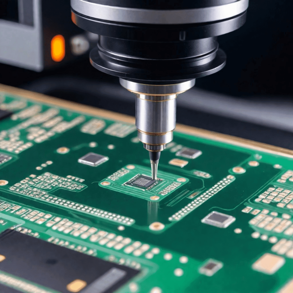
Understanding PCB X-ray Technology: A Game Changer in PCB Assembly
Application of X-ray inspection is vital in guaranteeing that PCBs are reliable and efficiently developed. This non-destructive testing proves useful since it supplements the direct vision of solder joints and electronic component placements through providing information on solder voids and bridges that the visible test cannot show This is a process whereby X-rays are passed through the PCB, and an image that captures any faults is taken through a detector. These are due to high accurate results, improvement in the quality of delivered work, affording favorable charges and intensive examination. The subsequent methods like 3D X-ray and Automated X-ray Inspection (AXI) increase the possibility of recognizing the defects and boost the elements for inspection making the X-ray technology essential in the contemporary manufacturing of PCBs.
Breaking Down the Science: Understanding Thermal Resistance PCB
Thermal resistance PCBs are significantly necessary used in the management of heat of the different devices in electronics, thus making the devices more powerful and durable. These PCBs employ materials with low thermal resistance, including Metallized PCBs, and apply some design practices, including the use of thermal vias, and heat sinks. Managing thermal resistance is a critical aspect of user interface design in preventing heat, reducing the likelihood of a device’s failure and increasing energy consumption. Through selecting the right material for the PCB to be used, controlling the thickness of the copper used, placing components in the correct manner, and integrating principles of advanced thermal management into the design, designers can come up with PCB designs that can handle the thermal performance associated with the high end applications that include automotive, aerospace, and high power electronics.
Crafting Quality Connections: A Deep Dive into Printed Circuit Boards Assembly Techniques and Best Practices
CCLs (Copper Clad Laminates) are essential for PCBs since they are a kind of dielectric materials containing copper foils. Fr4, Cem1 and Polyimide are some of these laminates that possess various characteristics including electrical insulation, thermal stability and mechanical strength making them adaptable to uses in many fields. Copper and other materials used in the manufacturing process include preparing the base resin and working on the copper laminates, laminating process, curing process and lastly inspection. CCLs are employed where devices, consumer electronics, automotive, telecommunication industries and various others require high reliability and flexibility. Knowledge of CCL types and property is important when deciding on which kind of material to use for a particular need in a PCB design.
Unveiling the Backbone of PCBs: A Comprehensive Guide to Copper Clad Laminates
Copper clad laminates also referred to as copper foil laminates or copper clad epoxy glass cloth provide both, dielectric support and copper conductive surface in production of printed circuit boards. There are different types of laminates and these are mainly designated as FR-4, CEM-1, CEM-3, Polyimide and Teflon laminates and these laminates are required to be used as per the application that they are likely to be subjected to, for instance electrical insulation, stability at high temperature or high mechanical strength. Some of the manufacturing operations carried in making of CCLs include preparation of base material, impregnation with thermosetting resins, lamination, heat conservation, cooling and inspection. CCLs is being used in electrical and electronics consumer goods, automobiles, communication equipment, industrial products, medical instruments, aerospace, and LED lighting application and many other sectors due to their cost-effective and reliable electrical and mechanical properties. As we have learned the different types and properties of CCLs above, one can easily choose the right material needed for the specific PCB design tasks.
Peeling Back the Layers: Understanding the Delamination Pcb and How to Prevent It
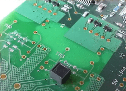
The delamination of the Printed Circuit Board (PCB) in the electronics area is a notable difficulty which influences the proper functioning and dependability of devices. This phenomenon often happens when the layers PCB start to come apart due to such reasons as high temperatures which occur during manufacturing process, the entrapment of water vapor, mechanical stress or chemical contamination. It reflects itself by noticeable marks, including bubbling and blistering when observing closely. As delamination does the material weakens, the PCB cannot perform its proper function, leading to defective products especially those which critical requirement might be there. To make sure materials do not delaminate, manufacturers should manage the lamination by well managed manufacturing process, handle and store materials correctly, take into account the geometry of parts that may eventually lead to stress, and carry out proper quality control testing and use high-quality materials. Viable methods like micro sectioning, thermal shock testing and acoustic microscopy are the needed tools to accurately assess delamination. Recycling is then executed by collecting the chip that is broken into small pieces, separating by color and quality, and an informative check which is proof of the chip functionality. Overcoming these obstacles is the key towards securing superior PCB of required standards.
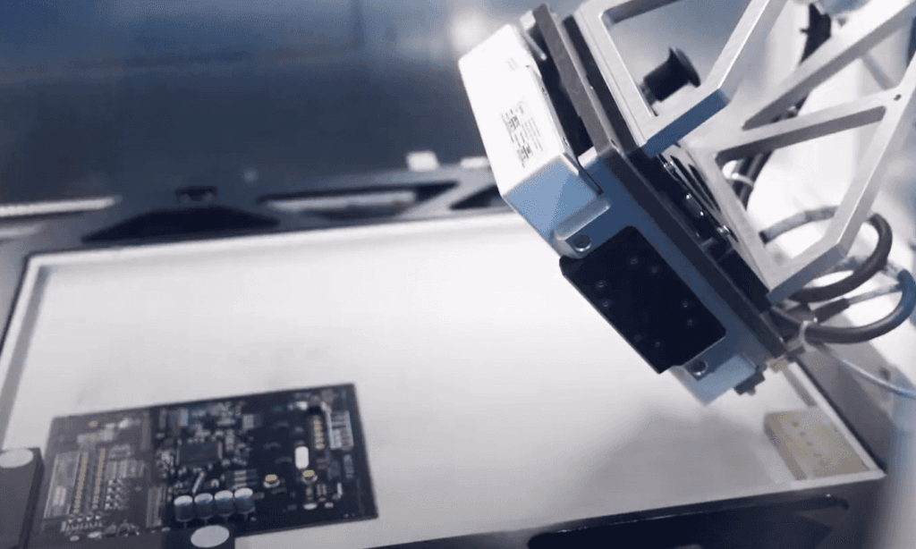
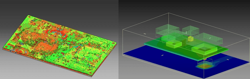
Shining a Light on Automated Optical Inspection: What You Need to Know
The document titled “Shining a Light on Automated Optical Inspection: In “What You Need to Know”, the author focuses on the importance of AOI in the electronics manufacturing as the AOI is utilized in modern electronics manufacturing. AOI systems are equipped with high-value camera configurations and lighting to inspect PCBs that will be in the framework of PCB making process. Guide highlights the ability of the AOI which determines the soldering errors, processing velocity of the PCBs and full fidelity as one of the features which exceed manual inspection methods. The integration of AOI in production lines is also covered and it is shown there one way is through the early elimination of quality errors that results in reduced rework and increased overall manufacturing efficiency. The technical documentation talks about both the technology’s scalability and cost efficacy, which makes it suitable for large scale production as well as it fits to anyone, whether it is simple or complex PCB design. Moreover, it offers the software and the hardware specifications of AOI systems, showing how they are integrated to maximize defect detection and to guarantee quality control. In the end, the document leads AOI to be not only an necessary tool in electronics manufacturing industry, but also a guard that brings forward advantages in quality and production efficiency.