Choosing the Right Substrate Materials: What You Need to Know
Soldermask is one of the essential processes in producing printed circuit boards, as it shields the copper traces on the board from getting rust, dust, and other electrical shorts that may make the board unusable. Retained time has a significant value for PCB due to the fact that it acts as an extra layer that prevents the PCB from coming into contact with certain environmental conditions. Moreover, soldermask enhances the aesthetics and makes the healing and diagnosing process easier since it provides a clear view of the solder pads and traces.
Blueprints to Bits: Mastering the Art of PCB Drawings for Efficient Circuit Design
In this course, learn how to produce a PCB assembly drawing that is a necessary step in designing and manufacturing printed circuit boards. The detailing of this scheme starts with developing a comprehensive diagram showing all the components and how they will be connected. After the placement of components on the board has been defined by design engineers, they then use PCB design software to create the layout, this with due consideration given to the arrangements of the components and the wiring of the electrical connections. Different steps in design are specifying the layer stack-up, putting the units so as to best cool the panel and reduce interference, and adding annotations which will guide to assembly. The providing of Gerber files is vital because such information is what a manufacturer uses to construct the printed circuit board (PCB) layers. Schematically assembly diagrams are created to help their understanding by showing them all the needed components placed on the both sides of the board. Careful, thorough work in the drawing, construction, and note-marking of the PCB assembly diagrams is to ensure that the design drawings are exact and useful, thus fostering smooth manufacturing and the successful building of the electronic components of the product.
Decoding PCB Design: Navigating Standard VIA Sizes for Seamless Circuit Connections
The article “Decoding PCB Design: The article titled, “Standard VIA Sizes for Afra-PCB Connection: A Guide to and Beyond” further explains why and how via sizes matter in PCB design. They learn about how the sizes of VIAs called diameter of the drilled hole and its related pad influences signal integrity, thermal management and how it can impact the manufacturing process. Standard VIA sizes are usually described in the range of 0 which would mean that companies have significant flexibility of choice. 2mm to 0. In this work, a new series of designs with dimensions of 5mm has been fabricated and discussed for their uses in the provision of secure electrical connections and heat sinks. It also guides users on which types of VIAs they should use through-hole, blind, or buried VIAs, as well as details step-by-step instructions on the best ways to select the correct sizes of VIAs by consulting industry standards, working with manufacturing partners, and design tools, as well as prototyping and testing. It is therefore important to gain adequate knowledge along with selecting the right sizes for the construction of VIAs in order to have optimal functionality, reliability, and design for manufacturing of the PCBs.
Unveiling the Power Within: Navigating the World of Circuit Board Capacitor
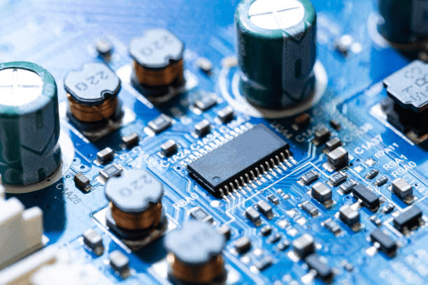
The article “Unveiling the Power Within: This article entitled “Circuit Board Capacitors: A Guide for Electrical Engineers” focuses mainly on how capacitors work and how they are applied into electrical systems because of their unique characteristic of storing and releasing electric energy effectively. Different categories of capacitors include electrolytic types of capacitors, ceramic, film, and tantalum, out of which the power supply use of filter capacitors, coupling capacitors, and timing capacitors is explained. The article also highlights the different markings used with capacitors and the best approach when it comes to selecting capacitors and using them on the PCBs, together with capacitance measurement of the PCB. Besides, it also explains how embedded capacitors with solid tantalum electrolyte are useful in increasing the density of the capacitors in the circuit boards and improve signal quality for high frequency applications. In succinct, the guide elucidates the importance of capacitors in ensuring optimal performance and efficiency of most electronics today.
Accelerating Innovation: Navigating the World of PCB Quick Turn Manufacturing
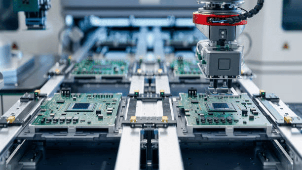
PCB quick turn manufacturing means the ability to provide printed circuit boards (PCBs) in a short time, this is very important for industries like telecommunication, automotive, and consumer electronics that require frequent changes of circuit boards for their products. Moved considerably within the product cycle to cut production time to make it easier for companies to issue their innovations to the market. Quick turn PCBs mean that a client would have a PCB developed within a short period to allow for immediate testing of other subsequent designs. It also employs cutting-edge technologies, automation in processes, and better organization to keep up high quality in combination with proper production rates. Being an innovation-friendly approach, this strategy also helps achieve competitive advantage and timely delivery to cater to customer’s needs in the market.
The Ultimate Guide to Obtaining Your PCB Certificate in 2024
This is a brief explanation of obtaining your PCB in the year 2024, according to the article entitled “The Ultimate Guide to Obtaining Your PCB Certificate in 2024”. It states that through the certification of printed circuit boards the company has confirmations like ISO 9001, RoHS, UL, and IPC. Some information basic on how to get these certifications includes the following; Understanding of the requirements towards getting the certifications, working with certified manufacturers, how to conduct an audit and how to maintain the certifications. Er discuses the advantages of the PCB Certification, which include ability to meet the legal requirement; improve the quality of its products; to satisfied its customers; and be able to competed favorably with other electronics companies. Acquiring these certifications makes sure that PCBs conform to the industries production standards and code of regulation hence enhancing their performance and viability most importantly to the consumers.
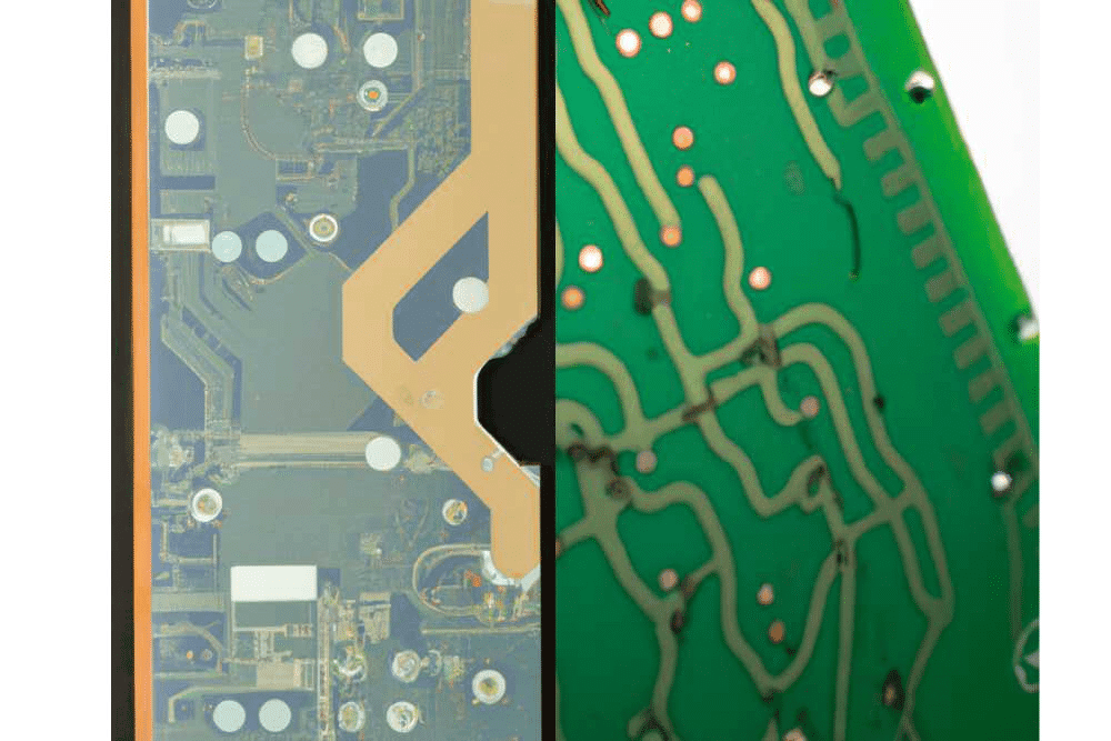
2 oz vs. 1 oz Copper Thickness: Which is Right for Your PCB Application?
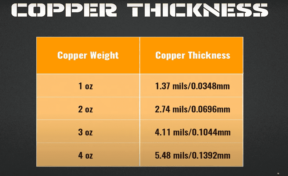
The article “2 oz vs. 1 oz Copper Thickness: ” “2 oz vs 1 oz Copper thickness in PCB Application?” compares the use of 2 oz and 1 oz copper thickness in printed circuit boards (PCBs), explaining the specific advantages and example uses of each. As a commentator for the provider of printed circuit board manufacturing services, it reveals the fact that the copper thickness measured in the ounce/square foot directly influences the conductivity, current density, thermal management capability, and reliability of the PCB. Though 1 oz copper is economical for general developing electronics and suitable for most consume electronics, 2 oz copper offering higher performance in every current and heat application such as power electronics, automotive electronics, and industrial control electronics. It all depends on things like today’s needs, thermal dissipating properties needed, current and available costs and manufacturing possibilities that direct design engineers to the most suitable copper thickness needed in specific PCB projects.
Maximizing Performance: The Impact of PCB Thickness on Your Design
The article “Maximizing Performance: Exploring the Technical Article “The effect of PCB Thickness on your Design” Here we are going to study one of the most important factors which behind the electronic device that is PCB thickness and its impact. What this paper seeks to do is to and expound on how the thickness of the PCB; the thickness of the substrate, thickness of copper layers, as well as the total board thickness influences mechanical rigidity, thermal convection, signal die and component compatibility. A brief outline of the standard thickness options of the main PCB types is provided in the article, including 0. 063 inches, 0. 093 inches, and 0. 125 inches and explained how those applications relate to their functionality. There is also information on how to select the thickness of RFID PCB and the common considerations such as thermal and costs. It becomes clear in this case to emphasize the need to achieve optimal PCB thickness for the appropriate durability and efficiency across numerous fields such as consumer electronics industries, automotive, and aerospace.
The Ultimate Guide to Protoboards: What They Are and How to Use Them
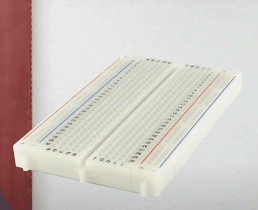
Prototyping on protoboards entails coming up with a circuit layout using a schematic, placing discrete components like resistors and Integrated Circuits onto the board, and interconnecting the components using conductive wires. This is done to provide the power and ground then the circuit is checked if it continues to work. It affords easy construction and qualified check with no soldering thus making the protoboards suitable for development and checking of circuits.
A Comprehensive Guide: What is Via in PCB?
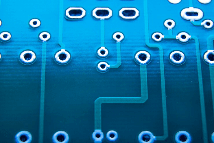
Vias on a printed circuit board (PCB) are structures that can be used in the connection of different levels of circuits or layers in order to transfer either signals or power from one element to another. There are various types of vias and these include blind vias, buried vias, through –hole vias and microvias though their function may slightly differ. They supply electrical paths, help with directing signals, cool/heat parts of the PCB and hold mechanical structure. These include drilling, plating, and sometimes even filling up the holes to provide conduction and strength to the drilled portions. High-density interconnects and Via-in-Pad technologies are setting the pace of PCB design in the near future the designers are coming up with new ideas and record for via integration to keep pace with the changes in the field of electronics.