In the matter of printed circuit board (PCB) design, vias are used to connect the components, which are separated by different layers of the board, and hence signal and power transmission from the components to each other can be done. This guide has aimed at clarifying the order of vias in the circuit board design and its types, uses, and professional practices.
Understanding Via in Printed Circuit Boards
Via are important components for designing and accomplishing a flawless printed circuit board (PCB). They are vital signal-carrying pathways that ensure electrical connection between different PCB layers and, therefore, the availability of signal, power, and ground planes. Vias are fundamental to modern PCB design by allowing the routing of tracks and utilizing space efficiently.
What is via in a PCB?
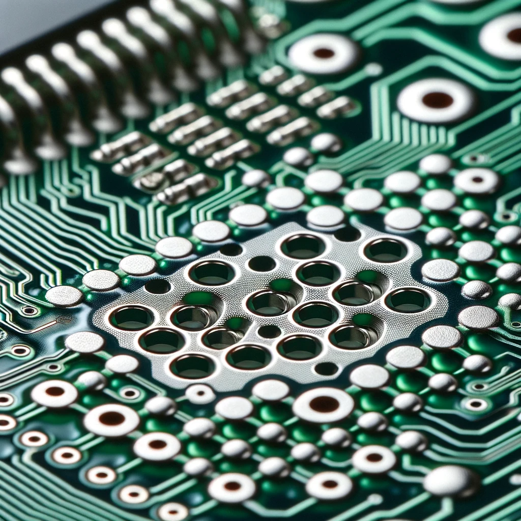
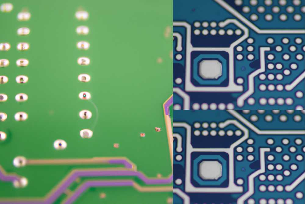
In PCB design, a “via” refers to a hole that is drilled through a printed circuit board (PCB) and is metallized to establish electrical connections between adjacent layers of the board.
Component Structure of a Via
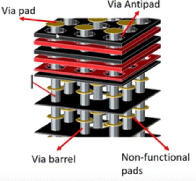
With reference to the case of PCB design, a via refers to a hole drilled to establish an electrical connection between internal and external layers of the printed circuit board. Here are the components of a via:
- Via Barrel: The through-hole that is conducted in the middle and unites the pins of the element together. It provides the current path from one layer that is drilled through to another layer through this conductor.
- Via Pad: It is also known in some cases as the annular ring partly, and it is this disk that is responsible for the electrical connection between the ends of the barrel and the traces or other components.
- Via Antipad: This is the deficit that is between the limb that is an appendage of the body and the one that is not a limb. However, due to absence of signal tracks the copper layer is a dead zone but it still ensures that no signal tracks can be made through the neighbouring plated holes.
Exploring Functionality and Purpose of PCB Vias
By exploring the functionality and purposes of Printed Circuit Board Vias:
- A. Electrical Connections Between Layers: The multilayer PCB will contain multiple circuit layers of electrical connectors known as PCB via, which offers signal and power trading through. Through-hole vias enable the continuous path of the transmission circuit that is imprinted on the surface of the board. Now, it possesses conductive midsection at each involved point, and/or at any time.
- B. Signal Routing and Transmission: PCB vias together with other forms of interconnections form a very important aspect of the routing and transmission of signals which cannot be underrated. They reduce signal attenuation, reflection, and emissions and increase the quality of the signal launched in high freq applications.
- C. Thermal Management: The PCB interconnect vias can be employed to manage or ameliorate the thermal issue of electronic devices in several ways; first, the heat source to be disperse the heat and, second, the level of exposure that operating component(s) can withstand.
- D. Mechanical Support and Stability: PCB vias can be used to add structural reinforcements features in order to help fixate the components and connectors into the board. It assists in the prevention of failure prompted by vibration, shock or maybe thermal expansion. Alongside, with the help of applying the soldering techniques, they ensure durability.
Types of PCB Vias
These are the types of PCB vias:
Internal layers of PCB Via
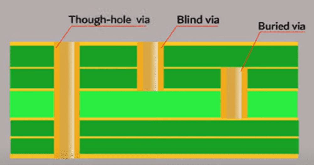
Blind Vias
Blind vias connect the internal layer(s) with the outer layer(s), but do not span the whole width of the PCB board. The head of the drill is from a certain side of the board and stops at a determined depth, enabling communication to the internal layers of the board without piercing through the whole board.
Buried Vias
Buried vias totally belong to the inner stack-up layers and never project to the outer layers. They form the bonds between the interior layers and are such that the dimension and outlook of the board are not distorted.
Through-Hole Vias
These are the conventional through-holes that go thoroughly through the printed circuit board from the top aspect to the bottom aspect. These are generally made by making openings in the board and then dipping the inside of the hole to make it conductive.
Microvias
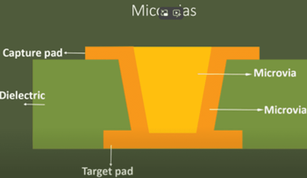
Microvias refer to narrow-diameter vias applied to high-density interconnect (HDI) PCB designs. They are available in either blind or buried formats and are manufactured either by laser-drilled or mechanical erosion methods. Microvias help to improve and shrink routing, and thus the component density on the PCB as well.
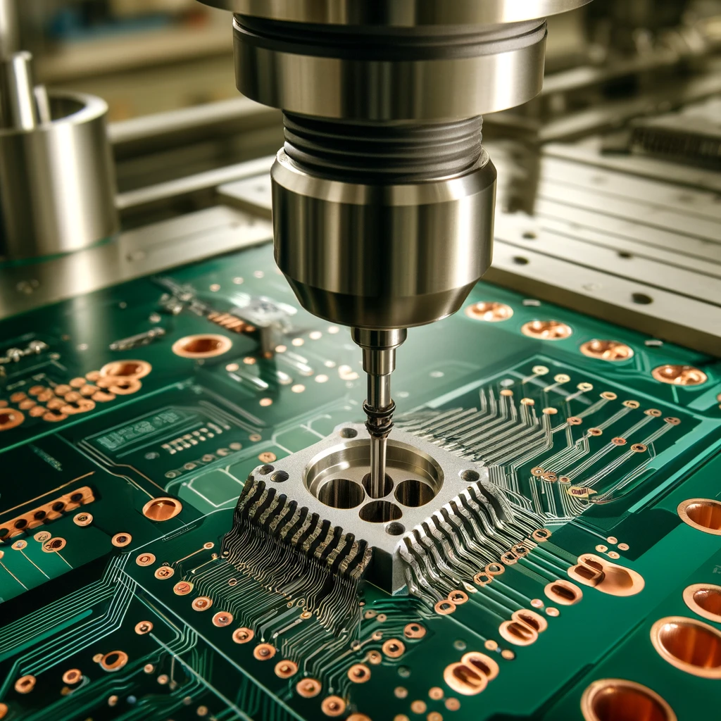
PCB Via Fabrication Process
Design and Layout: The process begins with a PCB design that engineers created via PCB software, where they plotted the exact location and routing of the vias. Relevant design factors, including signal integrity, thermal management, and PCB fabrication feasibility, are considered.
Drilling: In the case of the through-hole vias, drilling is the foremost process that leads to the formation of the holes. The automated drilling machines will be utilized for getting holes in the substrate and non-conductive material (usually fiberglass-reinforced composites), as determined by the settings in the design. In the case of holes being made smaller, drilling with lasers or with smaller tools is employed.
Plating: Once drilling is done, the inner walls of the vias will be coated with conductive items (such as copper) by either of the two plating techniques (electroplating or electroless plating). The plating development ensures the capability of electrical conductivity between layers.
Lamination: Multi-layer PCBs are the bondage between the layers that are laminated together using heat and pressure. This procedure guarantees good connector formation and the attachment of the vias to the surrounding layers.
Via Filling (Optional): In certain instances, vias can be filled with non-conductive epoxy resin to maintain the integrity of the product, thermal management, and signal quality. This process, called via filling, also accepts the name of via-in-pad technology.
Surface Finishing: The PCB surfaces are finished by a coating process (e.g., HASL, ENIG, OSP) so that no corrosion can occur, but solder mask would be more convenient and the reliability would be increased.
Testing and Inspection: As incredibly strict, high-level quality control plays a significant role in PCB production. A variety of laboratory tests for checking optics and electrical values are carried out to catch defects, make sure the vias are correctly connected, and confirm functional integrity.
Exploring PCB Vias in Advanced Technology
Emerging PCB technologies refer to a set of techniques and design engineering principles that increase the functioning, reliability, and ability to react in time for printed circuit boards (PCBs). Here are some key advanced PCB technologies:
- A. Via-in-Pad (VIP) Design: It is realized by the process of creating vias that are placed directly into the pads of surface mount components and is particularly beneficial for BGA (Ball Grid Array) bags that are in scope. VIP architecture through shorter transmission lines and better current flow
- B. Stacked Vias and Sequential Lamination: Through stacked vias, the functionalities of vias (interface conduits) are vertically layered on each other, which results in to a high-density interconnection. Sequential lamination is the practice of building several PCB layers in a sequential order, one layer on top of another, with staggered vias, ensuring signal integrity and decreasing electromagnetic interference (EMI).
- C. Skip Vias: Skip Vias is a computer-based via that allows the circuits to be connected at multiple layers but is not in any way connected to one specific layer. Mode selects specific way, which is either covered or hidden to exceed. The instances provided, vias 3-6, refer to the disjoining via that intersects four circuits with the connection of two circuits involved.
- D. Via Stitching and Shielding Vias: Through “via stitching” refers to where vias are hovered near the high-speed signal traces or power planes, aiming to lower radiated emissions and improve signal quality. Shielding vias work in the same manner as they form electromagnetic shields between sensitive portions or signals.
Design Considerations for PCB Vias
These are the design considerations for PCB via
A. Aspect Ratio and Diameter Considerations
A via’s ratio is an important measure of the relationship between its length and diameter for the designers to strike a balance between two things: reliability and PCB manufacturing, both of which present challenges.
B. Placement and Routing Guidelines
Proper channel placement is crucial for maintaining signal integrity. Place vias strategically to minimize signal reflections, crosstalk, and impedance variations. Use via stitching techniques for high-speed signals or critical analog/digital interfaces.
Connect power and ground planes using vias in PCB design to ensure low impedance paths and efficient return currents. Distribute vias evenly to minimize loop inductance and reduce EMI susceptibility.
C. Thermal Considerations
The location of critical engineering of the via is a crucial element for maintaining high-quality signal integrity. In the distribution of the vias, it is better to put them in places that reduce signal reflection, crosstalk, and impedance variation.
D. Signal Integrity and Impedance Control
The signals at high frequencies should be routed via controlled impedance vias to attain higher signal integrity and to avoid mismatched source and load impedances causing reflections. Opt for the design using dimensions and materials as per our own customized impedance levels to keep them as minimal as possible.
Application and Industry Use Cases
PCB vias are the essential components in modern electronics that cover a wide range of fields, including electronics, aviation, defense, telecommunication, household appliances and so on. From compact consumer devices to complex aerospace systems and life-saving medical equipment, vias contribute to the functionality, reliability, and performance of electronic systems.
- Consumer Electronics: Smartphones, tablets, laptops, PCs, wearable devices, and sensors all rely on microvias for tiny design, efficient signal routing, and condensing components with highest functionality while preserving the indelible space as well.
- Aerospace and Defense: Vias in PCBs are utilized in avionics systems, electronics for aerospace and military systems, signal routing and integrating the circuitry of communication devices, surveillance systems and missile systems.
- Automotive Electronics PCB: vias are essential in vehicle control systems and EVs, enhancing performance, safety, and connectivity and contributing to power distribution, battery management, and motor control.
- Medical Devices PCB: PCB vias are terribly important for diagnostic equipment and implants in medical devices, especially for accurate data collection and analysis and for the compact, reliable connections, which greatly matter to the challenging use as life safety functions.
- Industrial Automation: Vias play the role of crucial links in the industrial automation control systems and robotics applications connection; therefore, PLCs, sensors, actuators and communication interface signals work in the best performance.
Future Trends and Challenges in PCB Vias
These are the future trends and challenges in printed circuit board vias:
- A. Emerging Via Technologies
- High-Density Interconnect (HDI): Besides the fact that the HDI development on microvias increases the route density and the signal integrity of PCBs, which can be explained as the reasons why the tighter routings and higher component density come (11). Due to the fact that the engine production of HDI technology is best for making small and light-weighted applications,.
- Via-in-Pad (VIP): VIP technology is a well-suited method for the occupied area of the PCBs that uses the underfill of the blind or buried vias below with the components’ pads being on top, so a clearer transmission is certainly ensured. Compared to using traditional surface-mount devices in high-speed and high-frequency applications, impedance discontinuities are reduced when coFleX is used, which enhances effective heat dissipation.
- B. Thermal Management Advancements
- Thermal Vias: Squrred-out thermal vias on the printed circuit boards enable thermal pathways that enable the heat sources’ transport off the heat generators and ensure that components have longer lifespan.
- Via Filling: Apart from using the technologies as barrier materials, new fillers which have electrical or electrically conductive properties can also be developed in the near future. use of these types of fillers has an effect on the mechanical strength, reliability and thermal properties of the particular component. The impact of such intermediates is also enhanced in harsh surroundings.
Challenges and Opportunities Ahead
Design Complexity: At the same time, with HDI and VIP, the process of placing complex circuits on PCB yields. The designer has to design these circuits carefully, including simulation and validation, describing the signal quality, reliability, and manufacturability.
- Material Selection: The selection of materials that make up all the elemental materials of substrate materials, fill material of vias, and plating materials has great importance in the accomplishment of thermal and electrical requirements. Picking the correct type of material requires the right combination of performance, cost, and compatibility with manufacturing processes.
- Manufacturability: Small-scale electronics and emerging technologies are based on the use of the most accurate production methods, appropriate machine tools, and expert manpower. Manufacturers must fulfil their investment in advanced-level equipment and technical training to meet the problem of assembling excellent-quality PCBs with complicated via holes.
Conclusion
In the intricate world of printed circuit board (PCB) design, the role of vias cannot be overstated. These tiny conduits serve as the lifelines that connect different layers of a PCB, enabling the seamless flow of signals, power, and data essential for electronic devices’ functionality. PCB vias are crucial in design, facilitating electrical connections and optimizing space utilization. They serve various purposes, including signal routing, thermal management, and mechanical support. The fabrication process involves intricate steps, with advanced technologies like Via-in-Path (VIP) design shaping the future. Vias are used in various industries, contributing to product innovation and reliability. Future trends include HDI and VIP technologies, along with thermal management advancements.
Mastering PCB design and integration is crucial for innovation, efficiency, and reliability in electronic systems, as technology evolves and requires a deep understanding of its intricacies.