Thermal Vias: Enhancing PCB Performance and Reliability in High-Temperature Environments
The document titled “Thermal Vias: The “Improving PCB performance and reliability in high temperature applications through introduction of thermal Vias” paper deals with the key role played by the thermal vias in PCBs, especially in thermal management at high temperatures. Thermal vias, which are tiny holes having plated furnishes with conductive materials like copper, are located at the specific position of the hot components in order to facilitate their heat removal from the hot spots to the cooler areas or external heat sinks. The document mainly focuses on different types of thermal vias, i.e. through-hole, blind, buried, micro-vias, filled, stacked, and staggered vias, which basically serve as an improved version of electrical vias for heat management and PCB design optimization.
Also, the information deals with ways which can be used to manage thermal vias effectively by putting emphasis on appropriate layout and spacing that helps in heating dissipation and this makes sure that operating temperatures of the equipment remains normal and prevents overheating. As a result, performance and reliability of the electronic device components heavily benefit from this, and its lifetime additionally gets longer. Also, the thermal vias generate many smaller-sized and optimized PCB board layouts by allowing the placement of components without the fear of thermal problem. In a nutshell, the document fully explains the importance of thermal weaves as an essential component of PCB thermal management technology and discusses the way they diverge from the traditional approach. In the environment where thermal stability of devices is crucial, thermal vias play an increasingly vital role.
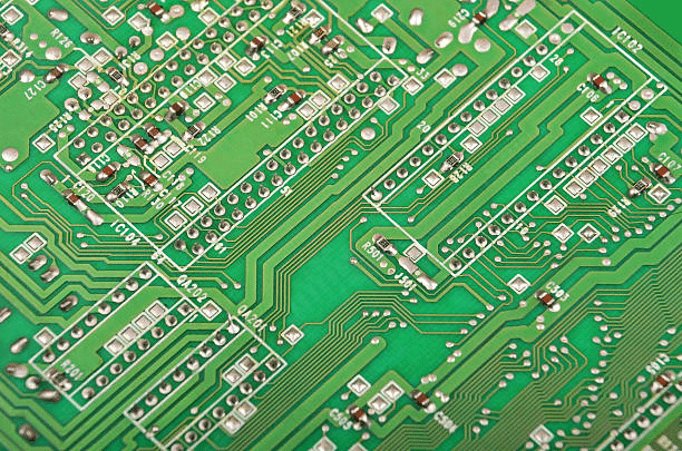
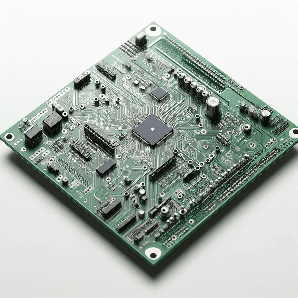
Decoding the Essentials: A Comprehensive Guide to the Parts of a Circuit Board
The article “Decoding the Essentials: One of the most instructive articles on the aspects of a circuit board is termed “A Comprehensive Guide to the Parts of a Circuit Board “(PCB). The online course aims to provide such people as students, hobbyists, and pros, with the necessary knowledge for them to work with electronics especially have silicon controlled rectifier. The guide goes through the substrate copper layers solder mask silkscreen and components vias pads ad traces which make up a PCB. Each component is a fundamental building block in building an electronic device, it is the signal boosting, storing of energy, and data processing making them so. Being familiar with these subjects enables you to design, maintain and repair your electronic components mounted gadget from a better perspective and, therefore, make this guide a learning tool suitable for use in enhancing your knowledge in electronics.
Mastering PCB Shielding: Techniques and Benefits Explored
An electronic device’s PCB (PCB) shielding proves to be really necessary in terms of the device’s functional quality and reliability because the shielding prevents EMI (electromagnetic interference). It can negatively influence device flexibility, affect the integrity of signals, and even cause the faults of components. The different techniques for shielding are implemented, including copper materials usage, catching for better PCB layout and shielded cans or conductive coatings are utilized to reduce such effect.
The concern about successful PCB enclosure mentions application areas like electronic products for customers, automobile systems, medical tools, and aerospace technology. These fields of applications involve rigid shielding cans which helps in minimizing the interference, which in turn enhances the device performance, regulation life and durability of the devices.
Implementing adequate rf shielding system while setting up a PCB design scheme will stop EMI interference which will later affect the overall functionality of the electronic system. Along this road, we focus on such aspects as the device’s dependability of application and also on the role that the EMC standards compliance play in avoiding both fines for penalties and product recalls.
What we discussed is only a brief introduction. More in-depth information can be found in the following resources OurPCB provided and other professional keyword.
Mastering Precision: The Ultimate Guide to Flying Probe Testing in PCB Manufacturing
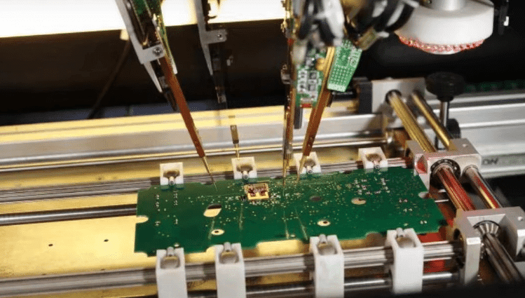
Flying probe testing is a widespread and problem-free approach that is widely used in manufacturing printed circuit boards to ensure quality and reliability. It provides numerous benefits compared to the bed-of-nails testing as the number of cavities is easily adjustable to comply with the production rate, the setup time is minimal, and it is capable to run even a single part or small production run with a sound economic foundation. An art in electronics involves positioning of movable touch probes from side to side and underside to test electrical connections and functionality by detecting traces and conducting paths. Though flying probe-testing is slower than other methods which makes it unfit for high-volume production, availing the exploration capabilities of its detailing as well as adaptability features, it becomes that which means most for the business when it comes to high-quality PCB. The final result is that flying probe testing can be very important in the manufacturing phase so that the problem of defects can be spotted early on and the trust and usefulness of the electronic products can be increased.
Designing for Excellence: Best Practices and Key rules for pcb design

From IOT and AI to different types of PCB manufacturing, the evolution of the design draws in all these advanced technologies as well as technologies that can improve the process of manufacturing PCB. And the deployment of these innovations is not only expanding the functionality and efficiency of PCBs but also clarifying that PCBs are indispensable devices in modern electronics also in through hole components. A computer’s printed circuit board should be created following well-structured procedures, which include gaining components and their libraries, proper placement of parts, and adhering to design rules and standards for a perfect signal route and manufacturing process. Nowadays, designers, together with software tools like Altium Designer and OrCAD, are able to successfully diagnose these conditions and implement the correct measures. These changes thus denote the ever-evolving characteristics of PCB design rules, which is always adjusting in a bid to address the need for demanding electronic functions.
Maximizing Performance: The Revolutionary Impact of High-Density Interconnect PCBs (HDI PCBs)
The recent HDI (high-density interconnect) circuit boards are fast becoming a vital part of circuit board design, especially now that we are witnessing this era, which requires the smallest space for high performance. Microvias, increased via density, fine-line technologies, and premium materials are some of the advanced features of these PCBs. These specialized PCBs have a high resistance to extreme conditions and crude handling practices due to their high-quality electricity performance and reliability. This diversity has created different grades of HDI PCBs of primary types, from the simplest enhancements to different applications to the unique complex requirements that high-precision aerospace applications and high-end medical technology have. Although they are more expensive to fabricate and take more time than their counterparts, HDI PCBs offer superior functionalities on the board in terms of density of components and signal integrity, thereby making the devices miniature in nature, which makes them an invariable part of future electronics.
Peering Into the Depths: The Essential Guide to Blind Via in PCB Design
In modern PCB design, blind vias are indispensable since the products are being made more complex and tiny with the advancements in technology. These vias are the roads that connect the outer layers to the inner layer or in copper layers ones without going through the entire board, giving several advantages such as space efficiency, better signal integrity, enhanced thermal management, and increased design flexibility to the buried vias blind. On the other hand, new materials are needed for the fabric of aircraft, which leads to higher final costs, increased design complexity, and troubles during the inspection and repair of these new materials. Manufacturing without-through hole vias technology is achieved by techniques that are dependent on the production requirements, either via mechanical drilled hole, laser drilling, or photo-defined vias. With the advancement of technology, the role of blind or buried vias and stacked micro vias is expected to increase, and this in turn will be the future of electronic design.
Unlocking the Versatility of PCBs: Exploring the Diverse Applications of Printed Circuit Boards
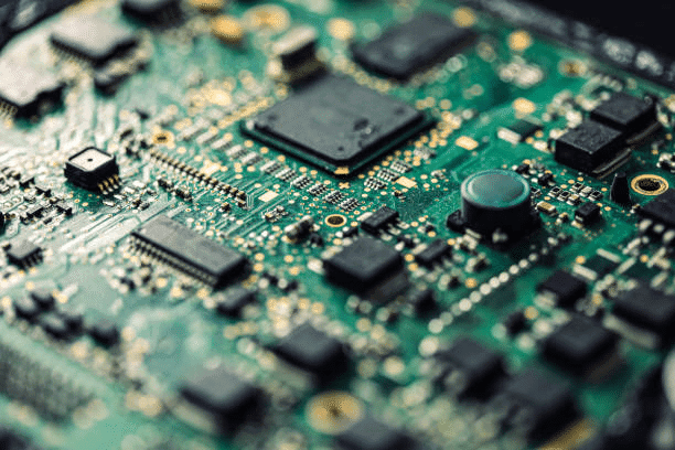
Printed Circuit Boards (PCBs) are among the essential components in electronic devices which not only confer them the mechanical support and electrical linkage of components through the conductive pattern etched from copper sheets but also contribute to most electronic miniaturization in the current electronics industry to the printed circuit assembly. These boards play a vital role in many of the fields such as consumer electronics, automotive and medical engineering, industry machinery, telecommunications, aerospace, and most exciting that is the Internet of Things (IoT). PCBs differ in type in an array from simple single-layer designs that err in their function than being affected by external conditions all the way to multilayer configurations with complex features to maximize the performance of specific tasks. The making process is one of the most challenging processes in engineering, because it involves many steps and requires a lot of precision, including the pcb design and layout, and the final pcb assembly. The correct usage and recycling going with the motion of eliminating health and environmental hazards comes as a result of the fact that PCBs might contain chemicals and heavy metals that pose as a health risk. While the technology is moving ahead at a breakneck speed, so is the application and import of PCBs, remaining key pillar in the status of the latest electronic devices.
Layered Precision: Unveiling the Power of Pre-Preg in Composite Manufacturing
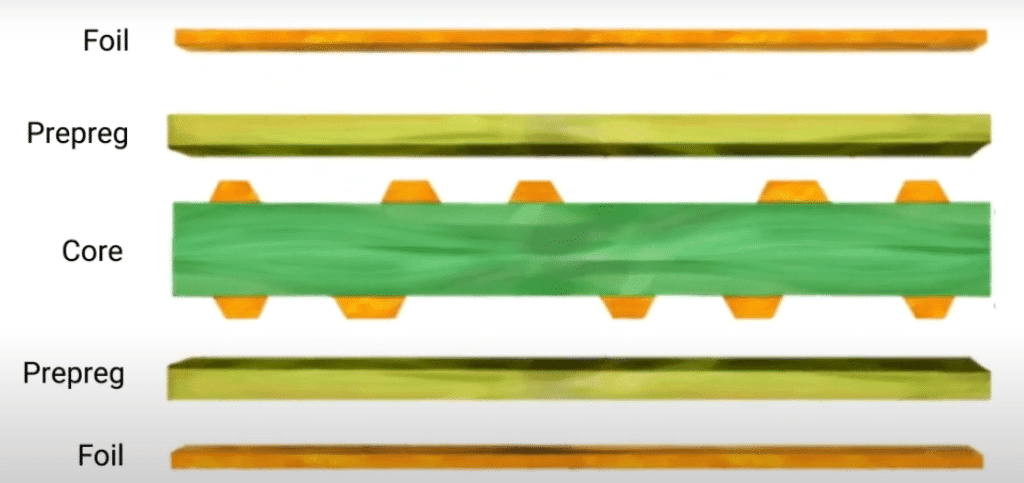
The blog “Layered Precision: “Explaining the Key Role of Pre-Preg in Composite Manufacturing” exposes the lynchpin role of pre-preg composites in modern manufacturing fields. Pre-pregs, which are the most common type of pre-impregnated materials, contain fibers like fiberglass, epoxy laminate, or carbon fiber that have been saturated and chemically bonded with an epoxy resin, allowing them to be molded into a final shape. The blog describes the manufacturing process in full detail, which consists of resin mixing, impregnation, calendaring, and curing. However, there is a need for precise execution at each step to obtain a high level of quality and optimal physical characteristics of the material.
The handout describes different varieties of PCB prepregs, e.g., standard epoxy, high-Tg, low-flow, etc., besides others, each of which is suitable to use for certain applications, like aeronautics, automotive, and high-speed digital technologies. In addition to this, it covers the topic of the two-way principle variation of prepregs and laminates, which is that even though the former acts as an adhesive for the multilayer PCBs, the latter produces the base structure.
Besides, the blog also discusses the benefits of using prepregs, such as uniform resin distribution, reduced voids, and easier process techniques. Nevertheless, it points out the pros and cons, including the high price, limited storage life, and the fact that the equipment is specially designed.
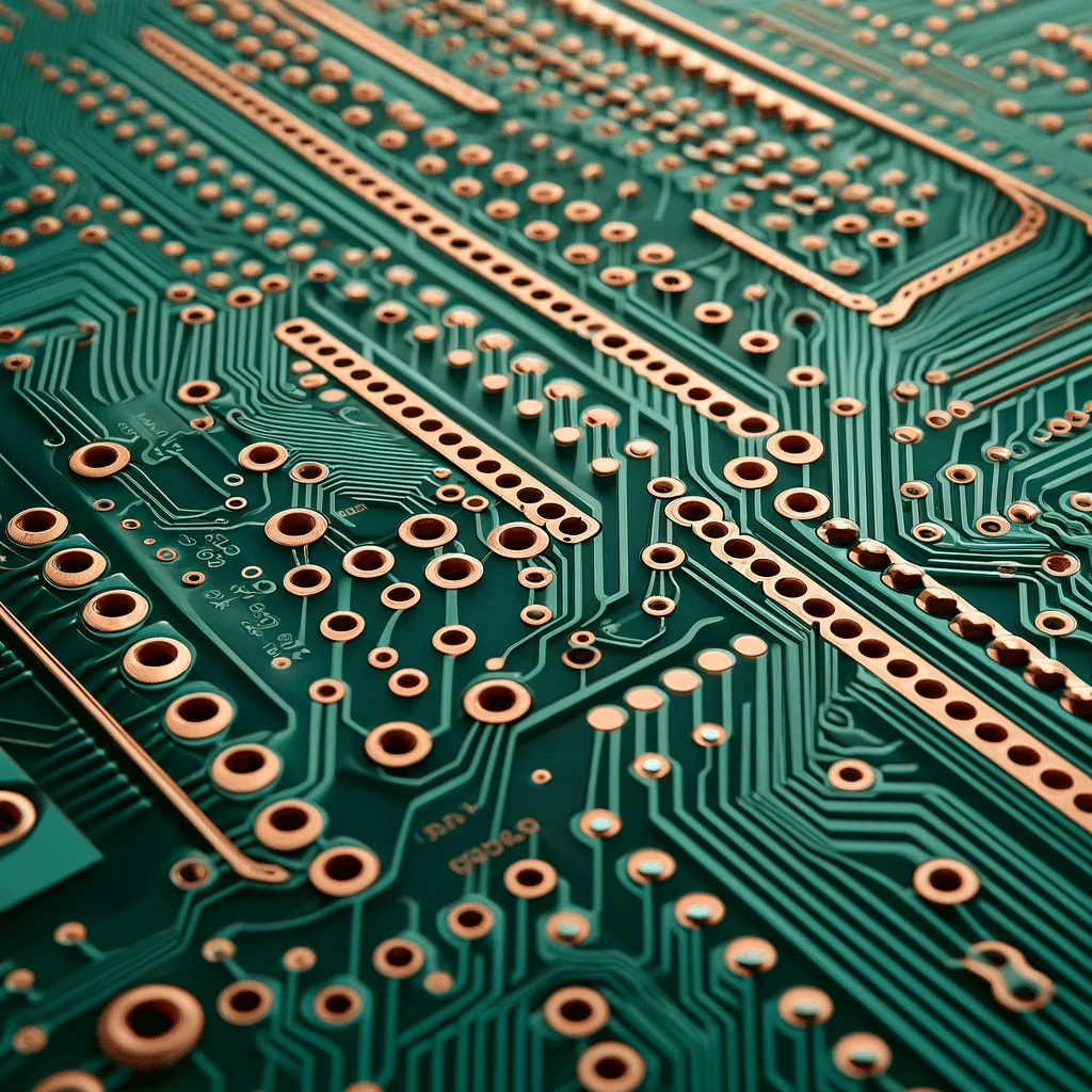
Understanding the pads in pcb: Their Role and Importance in Circuit Design
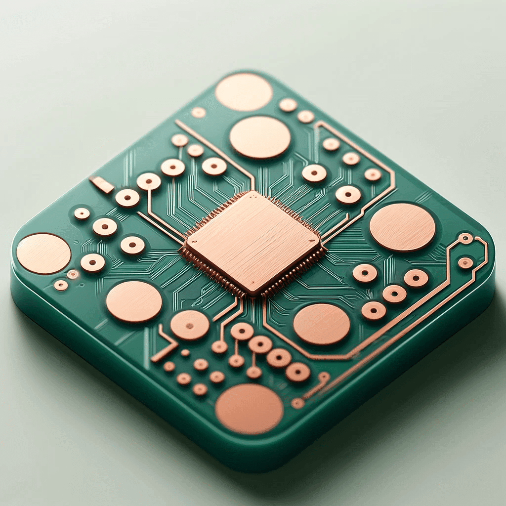
PCB pads represent the must-have features of the PCB, as they are the basic mount location of the components and are needed for soldering. These pads are created to offer the maximum level of reliability in the mechanics and electric company, as they are essential to the good function of the PCB to solder mask apertures. Solder pads need to be positioned and aligned properly to avoid joints that are too thin or solder connections that stagger over other pads, preventing good connections and compromising the PCB performance solder mask apertures applied. Specifically, pads currently in use are generally double-sided, one being through-hole and the other surface-mount, which are good for different assembly processes. Properly deciding the design of the PCB pads and roles of all electronic schematics is basically for durable and effective work.