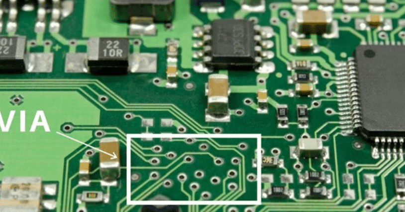
Step-by-Step: Integrating Via-in-Pad Structures into Your PCB Assembly Process
Implementing Via-in-Pad structures into your PCB assembly requires a step-by-step process that guarantees signals’ dependability and circuit performance. It begins at the design phase, where moreover with the locations of the vias within the pad areas they must everyone space effectively and provide the optimal electrical characteristics. After that, through maybe some intricate methods of drilling, the formation of the vias occurs, and then they set up copper plating to ensure the connections are good. Generic to all types of vias, appropriate filling of the cavity usually with conductive or non-conductive epoxy is important to eliminate solder voids during assembly. The copper is then electroplated as an under bump metallization for solderability and surface finished using ENIG. In the course of the process, the two procedures, inspection and testing are crucial in as much as they can provide the assurance that the vias created comply with the intended design parameters and as well can effectively function as expected in the final product.
The Ultimate Guide to Optimizing Your PCB Layout for Efficiency
Printed Circuit Boards (PCBs) are fundamental components in various electronic devices, constructed using different materials to optimize performance and durability. A PCB typically consists of a non-conductive substrate, often made from fiberglass or epoxy, with conductive copper paths that connect electronic components such as resistors, capacitors, and integrated circuits. Multilayer PCBs incorporate additional layers of dielectric materials, conductive layers, and surface finishes to enhance functionality. FR-4, a fiberglass-reinforced epoxy laminate, is the most common substrate material due to its excellent electrical insulation, mechanical strength, affordability, and ease of fabrication. Despite its advantages, FR-4 has limitations, such as lower heat resistance and potential environmental concerns. The choice of PCB materials depends on application requirements, environmental conditions, and performance expectations, balancing factors like thermal conductivity, mechanical strength, and cost.
PCB Board Material Breakdown: Understanding Properties and Applications
The document “PCB Board Material Breakdown: The writing titled “Understanding Properties and Applications” gives information concerning the materials used in the fabrication of the printed circuit boards (PCBs) and the role these materials play in the relevance of the technology. It starts with explaining what an PCB actually is, the non-conductive material it consists of like fiberglass or composite epoxy, or some other material and the copper tracks or conducting paths built on or inlayed on the surface. In this document it explains few of the PCB components they are resistors capacitors, integrated circuits, diodes and transistors; inductors and connectors; LEDs and switches; and, last but not least, crystal oscillators. It goes further to describe the substrates and conductors in multi-layer PCB, the dielectrics, surface and finish material, filler and the several types of PCB planes; the top plane, the bottom plane, the signaling plane, the power plane and the grounding plane. It is crucial for all the readers to understand the reintroduction as well as the advantages and disadvantages of the FR-4 material which is preferred by most producers due to its electrical insulation, mechanical strength, low cost, and easiness in processing before being conscious of its vulnerability to heat and its impacts on the environment. Last but not the least, the last section of the document presents a comprehensive analysis of hard and soft PCB substrate materials with offering the good and bad factors and the applications of them.
A Comprehensive Guide to PCB Standard Via Size
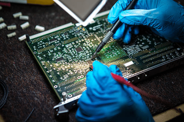
The complete manual for testing printed circuit boards presents various methods, which may be of considerable importance in determining the suitability of printed circuit boards that are used in electrical and electronic devices. It includes part-acquiring tests and simple tests such as visual optical inspection, though it also looked at the Advanced Optical Inspection (AOI), in-circuit test (ICT), functional test, and flying probe test. They include the details of the techniques themselves, the specific uses, efficiency, and drawbacks in each case, allowing designers and manufacturers to make the best choice when it comes to the implementation of PCB projects. The guide also points out that testing should be conducted effectively so as to prevent and identify certain defects, validate design, and ascertain the high structural quality of the final product.
The Ultimate Guide to PCB Testing Techniques

The basic purpose of the Basic Guide to PCB Testing Techniques is to give an outline of the numerous approaches that can be utilized to check the operational effectiveness of PCBs. Some of these techniques are Visual Inspection that helps in detecting any visible defects on the external surface of the board, In Circuit Testing that checks individual components of the board which may include resistors, capacitors, etc., and Functional Testing which determines the efficiency of the entire board once the components have been assembled. Some of the most sophisticated techniques which are used in the process of detecting hid denominations and soldering nodes are Automated Optical Inspection (AOI) and X-Ray Inspection. The guide also provides information on the kind of testing referred to as Flying Probe Testing that is appropriate for low-volume types of PCBs and Burn-In Testing, which is suitable for the assessment of PCBs’ reliability in extreme conditions. Following these techniques, one can adjust the strength, flexibility, and other desirable characteristics of PCBs and minimize failure rates.
Optimizing Efficiency: The Significance of PCB Standard panel sizes
Huge efforts should be made to pursue the standardization of the sizes of the panels to underscore the progressive improvement of efficiency in the electronics manufacturing industry. Pursuing the specific dimensions of panels has been beneficial in various ways, such as cutting costs on materials by reducing waste, enhancing the processes involved in production and ensuring the compatibility of equipment. Standard panel sizes like 18×24 inches, 21×24 inches, and 24×26 inches ease the benefits described above. This is even further enhanced by the practice of panelization, where numerous PCBs are built on a single large substrate. I learned that there are various methods of depanelizing, which include V-groove, tab routing, laser cutting, and depanelization saws, and that the choice of method to use depends on the required production parameters for the assembly line. In conclusion, the standardization of sizes of PCB panels is a plus for the fabrication of electronics since it minimizes quality issues, lower costs, and environmental effects.
The Ultimate Guide to Understanding Via Plating Thickness in PCBs
For more information on via plating think and the use of via plating in PCBs the article titled “The Ultimate Guide to Understanding Via Plating Thickness in PCBs” is a good place to start. It further goes deeper to detail out the various kinds of vias; through hole, blind, buried, microvias and their operational role in creating connection path across various layers of a PCB. The relation and intricacies of PCB via size and structure are highlighted with special focus on the plating thickness which plays a pivotal role in attaining the desired electrical conformance, mechanical strength and manufacturability. This article explains the methods for PCB plating like electroless copper plating and electroplating, immersion plating, other pros, and cons of plating thickness especially in the high aspect ratio via. It also covers some questions decisive for PCB reliability such as barrel cracks, the procedures necessary to avoid them and other matters concerning the proper functioning of PCBs for various uses in electronics.
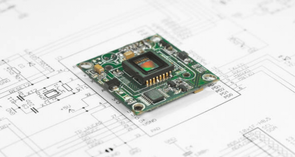
Innovative Types of Printed Circuit Boards: Revolutionizing Technology
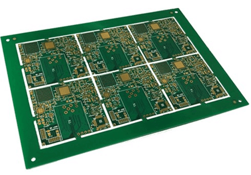
Evaluating printed circuit boards various roles as comprehensive backbone of mounting components in electronics, highlighting their importance in electronic circuits. There exists various varieties of PCBs which are designed for different uses; some of these are single sided, double sided, multi-layer, rigid, flexible, rigid-flex, high-frequency, HDI, metal-core, and aluminum-backed PCBs. All type have their specific advantages including the signal Integrity, heat sinking, and flexibility with the prospect that they can been used in consumer electronics, automobile, medical technology, aviation and telecommunications. Selecting the appropriate type is imperative by considering factors like functionality, available space, environmental conditions that the PCB is to endure and cost.
Expert Tips for Soldered PCBs: Enhance Your Electronics with Precision
Soldering of circuit boards involves placing and joining electronics components onto a printed circuit board (PCB) making use of solder which is defined as a fusible metal alloy. This aids in achieving strong electrical connections, and entails heating of the solder until a liquid like state that establishes connection with the component leads and the conductive tracks of the PCB is attained. Flux, solders, flux remover, solder wick, soldering iron, and solder paste are some of the materials used in the molding of solders in PCBs. The common soldering technologies involved are through-hole, surface mount, hand soldering, reflow, drag, selective, and wave soldering depending on various applications. Soldering is one of the most important practices in the assembling of electronic devices, as poor soldering is likely to lead to problems such as solder bridges, cold joints and wrongly positioned components as a result of inadequate preparation, improper technique and Royce’s 3 C’s, conformity control and cleanup.
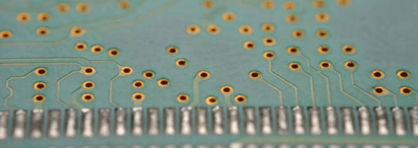
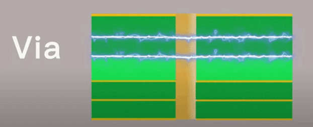
Into the Core: Understanding the Essence of PCB Vias
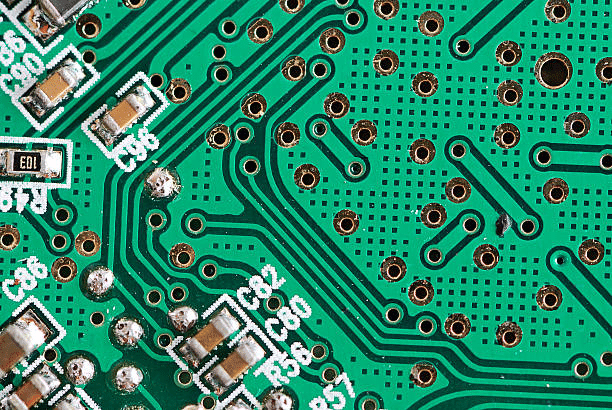
A PCB via is a small hole which has to be drilled through the printed circuit board in order to provide working connection between the top and the bottom layers of this board. These vias play an important role specifically for the multilayered PCB arrangement in order to allow the passing of the signals and power between layers. That is why there are through hole, blind, buried and microvias to meet numerous demands of the design. The vias greatly assist in the electrical connections, signal, thermal and component placement and therefore are critical elements to address in a reliable & efficient PCB design.