Vias are always more than just the tiniest of holes in PCBs, carrying with them the complexity of circuits. They are the essential building blocks that are placed underneath the top and bottom adjacent layers of carbon-based boards and act as contacts between them.
This blog will address the imminent importance of the vias and all types of designers might consider to manage the process of PCB design.
What are Vias?
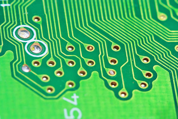
The via (the abbreviation of vertical interconnect access) creates a little hole in the PCB. A conductive material, such as metal, is used to fill or plate the hole. The signals of electricity go through it. Vias, both vertical and horizontal, allow not only vertical interconnection but further environmental control and signal integrity.
The Crucial Role of Vias-Printed Circuit Board
Through vias, pads are connected and the functions of circuit boards (PCBs) are shaped, affecting various key components of PCB optimization. Here’s a closer look at their crucial functions:
- Electrical Connectivity: The vials are used first and foremost to electrical connections link several layers of a PCB together. In multilayer PCBs with significant component density, holes allow signals to travel over the multiple layers. Hence, it serves as a crucial element for complex electronic circuits.
- Thermal Management: In the case of high-power electronic devices, heat dissipation is always a worthwhile problem. Vias act as heat conduction paths running away from components that can produce heavy amounts of heat, such as microprocessors and power transistors, towards less critical areas or external heat sinks.
- Enhancing Signal Integrity: In the case of high-speed systems that handle frequent signals, ensure the signal integrity is maintained to avoid performance issues. Through the use of vias that reduce signal loss and noise, users are allowed a chance to maintain the quality of the circuit board despite problems such as crosstalk and electromagnetic interference (EMI).
- Structural Integrity: Apart from their electrical and thermal roles, vias also add a bolt of sturdiness to a given PCB. These factors building up the overall strength of the board help it contain the PCBs even when they are undergoing extreme conditions, like extreme temperature cycles. This structural support is an inskipping feature for the sake of the PCB continuing to function properly within its intended lifetime of stresses and environmental exposures experienced during the process.
Types of Vias pcb layers
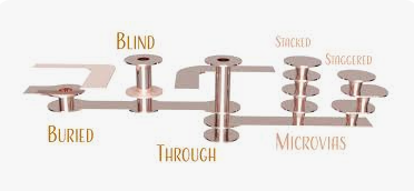
Vias constitute the essential elements of PCBs and are available in diverse types to comply with different design constraints and fabrics. We have three types of ones, among which are different from others because of their specific purpose and are chosen on the basis of layer connectivity needs, board size, density, and manufacturing capabilities. Here’s a detailed look at the common types of vias used in PCBs:
Through-Hole Vias pcb
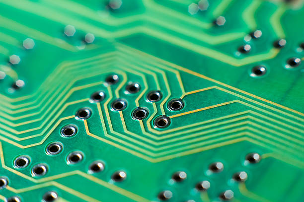
Traditional as they are, through-hole vias are the most widely used ones. These linear shapes interlace across the whole PCB manufacturing, from the top to the bottom layer. This type of via is very quick to fabricate and serves well as a line intersection between the many different board layers. Through-holes are commonly used in the manufacture of products where the placed components must stand the test of extensive use and time.
Blind Vias pcb
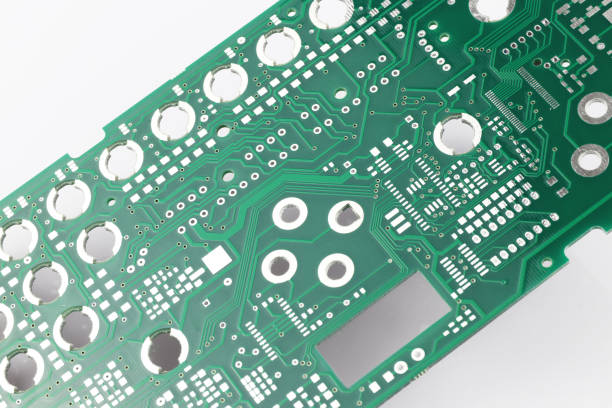
Going inside the layer, a long conductor hole or blind via starts on the outside layer of the same PCB and is terminated on the inside layer. There is no visible path from the opposite outer layers of the PCB; they are known as “blind.” These holes are utilized to save space on multilayer PCBs because they do not cover the whole of the PCB. Blind or buried vias are useful in densely stacked new models of PCBs where there is minimal available space and, consequently, for the stacked layer of printed circuit board components as they can be accommodated.
Buried Vias
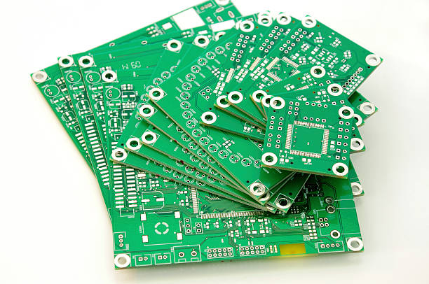
Buried vias are totally encapsulated in the printed circuit board to perform interconnection of inner conductor layers without outside conductor layers. These vias are employed with the view of achieving the objective of overcoming the problem involved in board density without violating the external lay-out plan. The buried vias designed for such boards are commonly employed in complicated, space-critical designs.
Microvias
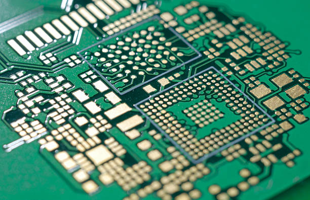
Vias in microvias are less than 100 micrometers in diameter, which means the smallest viable diameter is closer to 150 micrometers. Liquid crystal ones are fabricated with laser drilling technology and are mainly applicable to high-density interconnect (HDI) PCBs. Microvias can strive for only a few layers and may be placed one after the other or on the contrary in order to provide vertical connections in a limited surface area. This is essential for the development of microscopic electronics such as miniaturized devices.
Filled Vias
Copper or silver is the conductive agent, and the drill line is passed through entirely or partially. The entire line is filled with a conductive material called silver or copper. Vias packing can advance thermal and power efficiency for PCBs, as well as strengthen the structure. The filled vias are gently utilized where surface flatness is a main factor; otherwise, the board becomes expensive. For example, in thermal management applications and in printed circuit boards with BGA (ball grid array) packages,.
Stacked Vias
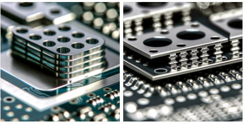
Vias are stacked microvias: consecutive vertical vias on the same level but at different stages. This kind of via cutting most often finds application for ultra-high-density designs with minimum space allotment.
Staggered Vias
Staggering micro-vias obviates 100% horizontal connection between metal layers but rather enables different orientations that retain the entire stack structure. This prevents the necessity of drilling as many holes as the microvia alone can fill. At the same time, it eliminates the requirement of complicated precision alignment of adjacent vias.
Design Considerations for Via in PCB
Designing vias in PCBs involves several key considerations to optimize performance, manufacturability, and reliability:
- Size and Placement: Decide whether thin or thick wires would be suitable in respective track diameters and spacing to manage electrical resistance, signal path length and thermal conductivity, without the circuit being crowded.
- Type of Via: Choose the kind of via (through-hole, blind, buried, microvia) that will suit your complexity, density, and those that will meet the PCB requirements.
- Thermal and Electrical Performance: Make use of vias to get ferocious heat dissipation and prevent their interference on the signal properties that might be caused by the inductance of high speed circuits.
- Material and Filling: For example, you can aim at the use of either conductive or non-conductive fills to get increased performance and excellent capability of thermal conductivity. Use spread for boards to protect vias from the environment.
- Reliability Concerns: The vias must be designed to protect from the harsh environmental conditions and have a high tolerance for mechanical stresses such as temperature cycles.
- Cost and Manufacturability: Match such designs with manufacturing capacities in order to mitigate costs and remaining on DFM (Design for Manufacturability) guidelines.
Through addressing these aspects you can improve the performance of your PCBs besides ensuring good quality items at a low production costs.
What is a Via-in-Page Design?

Through-Hole Technology in Pad design is a layout method where vias, placed directly under a component pad. This enables reducing the area occupied by the traces, provides high signal-integrity levels, and generates good heat dissipation conditions during annular ring.
The Advantages of Via-in-pad
Via-in-pad design offers several advantages:Via-in-pad design offers several advantages:
- Space Efficiency: Include vias inside the component pads of the PCB as it will save the PCB space, which is then sufficient and compact.
- Enhanced Signal Integrity: Smaller vias decrease the signal paths length realizing signal power loss and degradation which negatively affect the performance of the signal integrity especially in high-speed and high-frequency applications.
- Improved Thermal Management: By metallurgically bonding the component lead-frame pads to internal layers through vias, this provides an efficient heat dissipation system which is vital for processors and power devices producing heat.
- Reduced Electromagnetic Interference (EMI): According to the studies that the shorter the trace tracks and the less the round of loops lead to EMI reduction, grants a better EMC.
- Higher Routing Density: Vias in pads have helped to improve PCB assembly routing as designers have a wider liberty to design traces that will connect the components of the circuit in a denser and more complex manner.
- Facilitates HDI (High-Density Interconnect) Designs: Multilayer technology set up via interconnecting-pad is common in the HDI designs and makes it possible to join fine-pitched ICs and multiple layers in smaller sized designs.
Via Aspect Ratio
As for a PCB via aspect ratio is the relation of the Dt and its r the depth and the diameter. It’s a critical factor that influences the manufacturability and reliability of vias:
- Manufacturing Challenges: Highly skew dimensions make this process challenging, especially when applying a positive amount of solder mask across the inner aspect of the via. This could result in an incomplete connection or an open circuit.
- Reliability Concerns: High bench Lycos and longitudinal stress may occur in veins with high aspect ratios due to the thermal expansion and contraction of the heat-treated silicon.
- Typical Values: In general, this is so because the aspect ratio remains less than 10:1 or even equal to 10:1, in order to provide a better impregnation, especially for thicker boards.
- Advanced Manufacturing: On the other hand, some manufacturers can deal with high aspect ratios (15:1 at most) by employing specific tooling, nevertheless, this often leads to higher costs and more rigorous design and inspection approaches.
When to Use Smaller Vias

Smaller vias are often used in PCB design under specific conditions to improve board performance, density, and integration:
- High-Density Designs: The smaller via in limited board space helps to maximize the open area to add components, e.g. in high-density interconnect (HDI) designs. Consequently, designing custom PCB fabrication enables solving a wide range of issues and enables fabrications of high-quality circuit boards that can be successfully used in all kinds of applications.
- Fine-Pitch Components: Fabrication procedures for parts such as BGAs (Ball Grid Arrays) are ruled by very fine pitch and smaller vias must be used to make the via compatible with the marked pad size and prevent shortages.
- Multi-layer Boards: Vias of the complex multi-layer PCB can be made smaller than the uneven pass where to connect a group of layers like inner and outer layers not penetrating the through of the board leaving space for other routing needs.
- Improved Impedance Control: In high-speed circuit designs, it is a small-sized via that can contribute to this reduction of the impedance discontinuities, the signal integrity improvement and noise reduction as well as cross-talk prevention.
- Thermal Management: The thicknesses of the holes can be customized according to the needs – the larger vias being generally preferable for heat transfer and the smaller holes being suitable for heat transfer as long as they take up little space.
- Aesthetic Reasons: Aesthetics is one of the key factors in choosing the price of a consumer electronics product that have the electrical connection board part seen on the outside. Hence, smaller vias make the board look slimmer and more compracble.
Route Signals with Vias
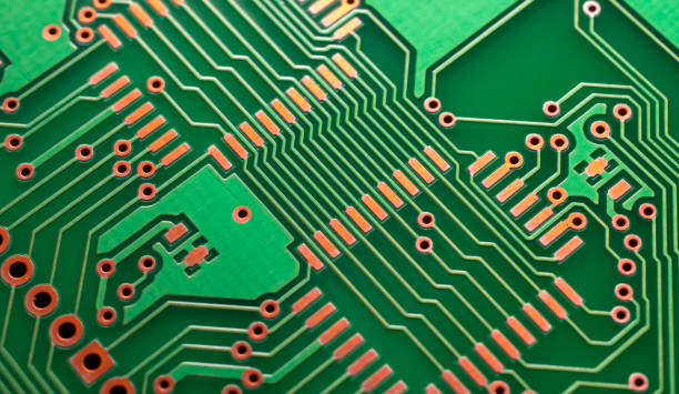
- Maximize the routing designs by reducing or eliminating vias to prevent potential loss of signal integrity.
- Use Via to shift between different layers on a multi-layer board, shortening and becoming more direct.
- Keep vias off of component pads by avoiding over-crowding unless you use the via-in-pad technology, as this can lead to soldering problems.
Conclusion
Vias are indispensable in the design and function of modern PCBs. They provide not only the necessary electrical and thermal current but also contribute significantly to the overall reliability and performance of electronic devices and copper plating. Understanding the different types of vias and their applications allows designers to create more efficient, compact, and robust electronic products. As technology continues to advance, the role of vias in PCB design is only set to become more pivotal, pushing the boundaries of what is possible in electronic design using different pcb layers.

