Discover the secrets of printed circuit board design with our complete guide! Plunge into deeper layers using plating thickness to gain knowledge on how it will affect circuit performance and reliability. Discover how you can harness professional techniques to standardize your plating thickness based on your specific application requirements. Uncover the nuances of the process, learn useful tips for your job and master the art to your enjoyment and satisfaction. Regardless of whether you are a pro or a freshman designer, this guide is going to be your must-have guide for PCB design.
What is a PCB via?

A Via PCBs, also known as “printed circuit board vias,” are a group of copper sections drilled through various levels of a printed circuit board (PCB) to make a connection. Vias, also known as holes, help to establish electrical contacts between the conducting layers in a PCB so that signals, power, and ground can be routed through the board. In short, they perform the role of an electrical conduit, through which the signals can send their data from the multiple layers of the PCB unobstructed. Vias can be classified into different classes and types depending on their construction purpose, e.g., plated through-holes (PTHs) and surface-mounted vias (SMVs). They are very important in the design of today’s PCBs because they enable the development of circuit boards with multiple layers of connections.
Types of PCB Vias
Vias in PCBs are a fundamental feature of printed circuit board (PCB) design, catering for inter-layer electrical connections. Here are some common types of PCB vias:
Through-Hole Vias (PTH, Plated Through-Hole):
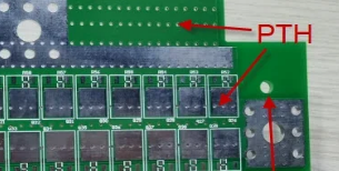
- These through holes, which are drilled into the entire thickness of the PCB, are plated with metal to create conductivity along the layers. Generally, they can be seen on double-sided and multi-layer boards.
Blind Vias:
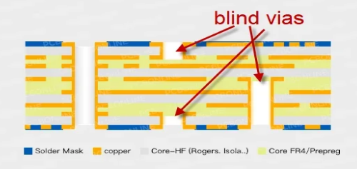
- Blind vias vertically integrate the outermost layer(s) with one or more internal layers; however, these are not penetrable by the entirety of the board. They exist only on the front side of the printed circuit board.
Buried Vias:
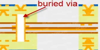
- Running vias link the inner layers of a PCB while not extending to the outer layers. They are hidden on the inner surface, which is not visible from the outer layers of the PCB.
Microvias:

- The microvias are small openings with diameters less than 150 μm. They are used in high-density interconnect (HDI) PCBs as a facilitation of connections between layers for complicated and tiny designs.
Blind/Buried/Microvias:
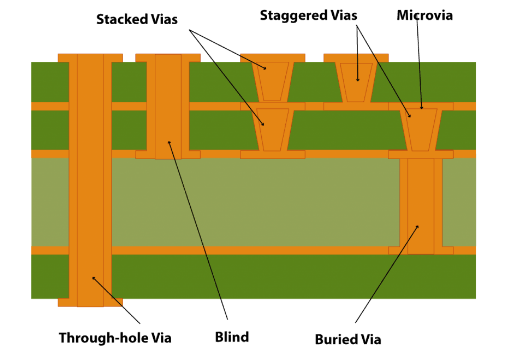
- These vias combine the features of blind and buried vias with microvias, which, in turn, permit high packing density and exact connection between any layers of multilayer PCBs.
Via-in-Pad (VIP):
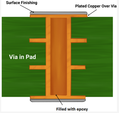
- Via in pad technology refers to the process of mounting the via to the component pads on the circuit board. This approach offers more space and improves the routing density, especially in fine-pitch surface mount technology (SMT) implementations.
PCB Via Structure
The building of a PCB via suggests to its physical building along with how it is included in the printed circuit board.Here’s a breakdown of the typical structure of a board housing a PCB via:
Drill Hole:
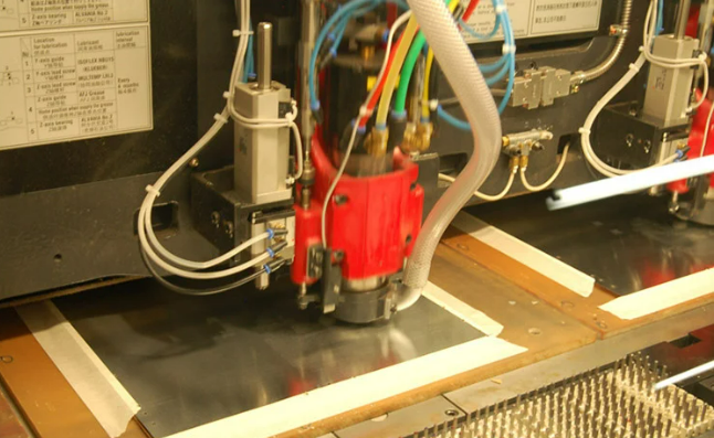
- In this via form, a drilled-through hole is provided in the PCB substrate. The hole size depends on the via type and design specification.
Plating:

- After the drilling stage, the PCB would normally go through the plating process, where the holes are coated with a conductive material such as copper. This is to provide electrical connectivity between different layers of the PCB. This method of plating is either chemical deposition-based or electroplating-based, which is the first PCB plating process.
Annular Ring:
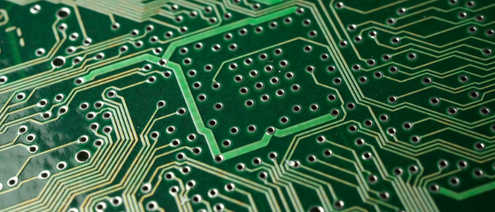
- Around the drilled holes on the flat outside layers of the PCB board, there may be a copper strip, known as the annular ring. This area serves as both the solder pad for connecting components and a pad to connect vias.
Barrel:
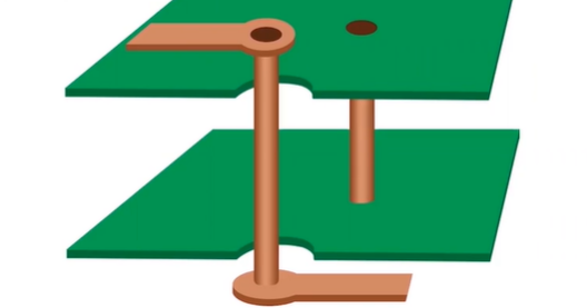
- The plated hole, together with a material that is conductive, forms the barrel of the via. The barrel passes through the entire PCB thickness in the case of the through-hole vias, whereas this thickness is only partially for the blind or buried vias.
Pad or landing pad:
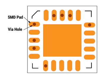
- On every layer of the PCB, the via is connected to the lands of a conductive pad. These pads, in turn, act as the conduit for making electrical connections with the tracks or components on the PCB.
Solder Mask:
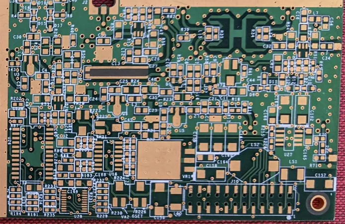
- A solder mask is applied over the PCB to ensure that conductive traces and pads are covered, leaving the vias visible for soldering. solder mask provides shielding that prevents unneeded solder bridging during the assembly, besides sheltering the PCB from its surroundings.
- Optional Features:
- Depending on the given design requirements, one or more features, such as via filling, capping or trenching, may be applied. Filling (which involves covering the plated hole with a non-conductive material) improves reliability and mechanical strength. The screen is capped by closing the via with a protective layer, while the entire via is tented under solder mask to avoid solder flow.
In general, a well-designed PCB via should be able to offer reliable electrical connections on different PCB layers and yet have the feature of being mechanically strong, maintaining signal integrity, and being manufacturable. Another factor is that different types of vias often have unique variations in their build to satisfy specific layout conditions.
PCB Via Size

A via on PCB means its diameter or area fills a small circular space which is drilled in the area where the need for a jumper is. The via size is generally picked according to the requirements of the specific design and the manufacturing constraints of the printed circuit board. Here’s a breakdown of the different aspects of PCB via size:
Drill Diameter:
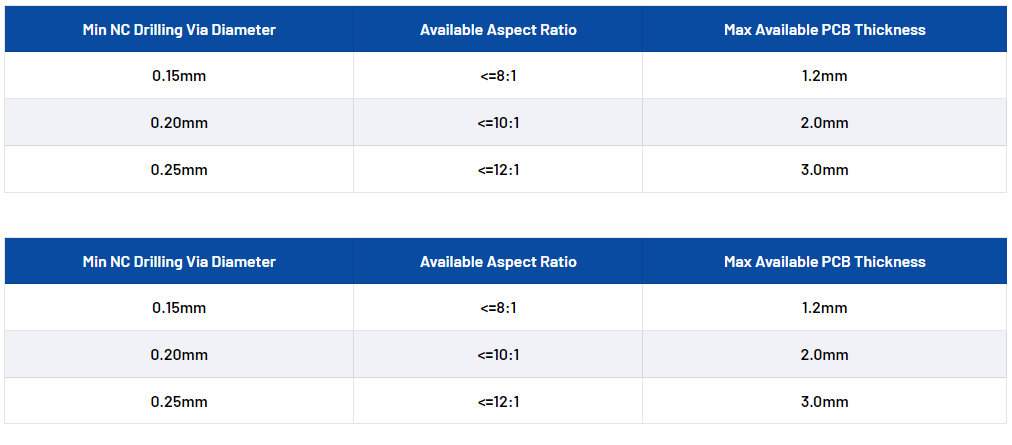
- The drill diameter is the width of the hole that is drilled in which through the PCB substrate will be created to form a connection. The diameter of the drill shall be determined by the types of holes in the PCB (through-hole, blind, buried, and microvia), as well as the stackup of layers and the drilling capabilities of the PCB fabrication facility. The diameter of the vias typically ranges from a barely visible 0.1 mm up to the great size of several millimeters, which is for through-hole vias.
- Annular Ring Width:
- The outer circuit edge of the PCB is marked by the annular ring, which is an electric copper pad that surrounds the drilled hole. Its inch is often quoted to create good soldering and a qualified connection as well. The width of the annular ring is determined by the drill diameter, traces and pads pitch and the manufacturing tolerance. However, the instructions for PCB design normally come in the form of PCB design guidelines provided by the manufacturer.
- Aspect Ratio:
- Aspect ratio is the ratio of a typical via’s depth (length) to its diameter. One of the crucial features is designability, which plays a big part when the board should have high levels of integration. High aspect ratios (ex., vias with a small drill diameter and thicker PCBs) may be causing some difficulties during the drilling, plating, and reliability checking because there are no fences between them. Producers may be limited by the feature aperture size of their machines as to the to the maximum aspect ratio they can incorporate sustainably.
- Finished Via Size:
- The via size, after plating and processing, talks about the size of the size of the drills and holes on the printed circuit board design. It consists of the drill diameter, the annular width, and aftermarket (via filling or capping) features.
- Minimum Via Size:
- The PCB makers normally stipulate the minimum diameter that will deliver the desired result in vias (holes). The small-size limitation is a function of the range of equipment that is used in the fabrication process, such as the drill diameter, thickness of plating, and registration thickness of the solder mask.
The allocation of PCB vias size is one of the most important considerations to be carefully considered ensure the electrical performance, signal integrity, reliability and manufacturability of the PCB with regard to the printing circuit board (PCB). The designers are to make specifications with particular consideration to the factors and should also adhere to the manufacturer’s guidelines when giving device via sizes through the etched board layout.
Annular Ring and IPC requirements
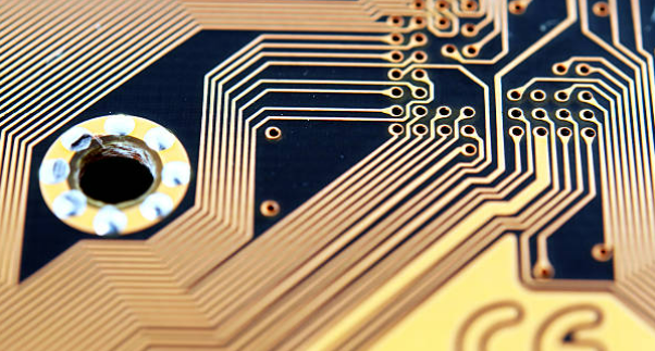
A printed circuit board (PCB) layer outside has an annular ring around the drilled hole composed of copper pad on it. It is a main part of the PCB structure; it needs to be attached so that the components can be soldered to it or connections can be made through holes in it. The smaller thickness of copper surrounding annular ring is crucial for having the good quality interconnections and solder joints and to ensure the efficiency of the electric current transfer. IPC (Integrated Production Cabo Design) draws up standards and expectations for each product’s PCB design, which includes annular ring specifications.
IPC-2221B (IEEE Standard for Printed Board Design) gives standard to be followed in designing printed circuit boards. This process, also known as public input process or citizen participation process, includes recommendations on the opening size and copper thickness of annular rings. This opening is based on the size of board house that a drilled hole is going to penetrate through (drill diameter) and according to tolerance levels of the fabrication process. The annular ring thickness is quite often stated as a minimum width at the rung hole edge.
Here are some general guidelines for annular ring size according to IPC-2221B:
Minimum Annular Ring Width:
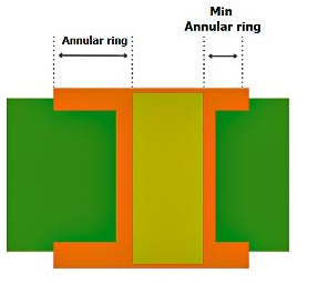
- The minimum annular ring width dimension, which is typically a percentage of drill diameter, is the most recommended characteristic in the minimum standard specifications. Likewise, IPC-2221B may require that the outer layer of the drill should never be less than 0.075 mm (3 mils) or 6 percent of the drill diameter, whichever is more.
Tolerance:
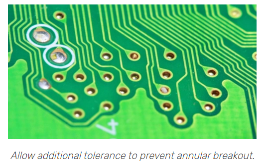
- The IPC standards also handle tolerances in annular ring sizes as an allowance for manufacturing discrepancies. Thus, the images and symbolism serve as potent tools to breathe life into historical events and enhance our understanding of the past. Engineers must check up that designers follow the singing annular ring width rule to obtain a high-quality solder and electrical connection.
Application-Specific Requirements:

- Beyond common IPC guidelines, particular manufacturing settings or application-based design specifications might cause an increase of annular ring size for more robust connection or a decrease of size for compact, high-density designs. While designing the annular ring, the designers need to be aware of the thermal stress, amperage capabilities, and manufacturability factors so as to calculate the appropriate annular ring size.
It is critical that PCB designers refer to the latest IPC standards and directives that are linked to their respective application and offer the correct methods of production for maximum reliability. Moreover, working together with vendors and other layers of the PCB fabrication and assembly chains will aid in ensuring that the selected annular rings sizes are in line with their manufacturing capabilities and are of related quality.
PCB Aspect Ratio and Via Plating
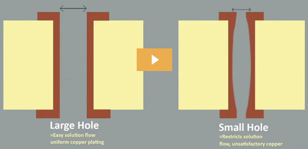
The aspect ratio in PCB design is the ratio of the thickness of the PCB board to the diameter of the hole in which the vias are made. Indeed, it is probably the most important parameter in assessing the manufacturability and reliability of the printed circuit board and definitely must compete with high-density designs or with fine-pitch components. That concerns aspect ratio restrictions specifically related to the process of plating for vias and the drilling process, which becomes more difficult with higher aspect ratio and can negatively change other properties of the vias and the quality of the circuitry itself.
How aspect ratio relates to via plating
Aspect Ratio Definition:

- The aspect ratio is calculated by dividing the PCB thickness by the hole diameter after drilling. The number of array operations is determined by the shapes and their aspect ratios. For example, if the board of the circuit thickness is 1.6 mm and the drilled hole diameter is 0.3 mm, the aspect ratio is 5.33 (1.6 mm / 0.3 mm).
Impact on Plating:

- The plating process is sensitive to higher aspect ratios and may cause challenges. Through electroplating, the copper is deposited within holes into the formed pathways to become a conductive current. On the contrary, as the aspect ratio increases, it is harder to plate the hole consistently through the whole of it. A single layer of iron can be incomplete or have a burr that leads to uneven plating, voids, or even complete plating failure in extreme cases.
Plating Thickness Considerations:
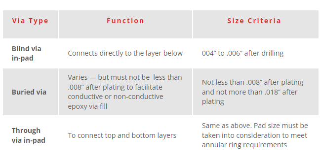
- The plating thickness needs to be large enough to ensure high electrical conductivity and mechanical strength. Utilizing etching processes with resists results in low aspect ratio vias; however, for distributed vias, uniformity of plating thickness might be difficult to achieve. Manufactory may need to habituate plating conditions or use special skills to be certain that coverage and depth are decent-quality.
Aspect Ratio Limits:
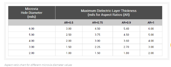
- PCB manufacturers usually have a limit on the largest aspect ratio they can handle ata given time. It needs to be related to PCB material properties, plating procedures, and the technology applied. Breaching the ratios higher than recommended can create the possibility of errors arising during the manufacturing process and life-cycle longevity problems.
Design Considerations:
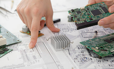
- The designers must meticulously contemplate aspect ratio limits and specifically these complicated constructions on the boards that have a higher density or are multilayered. Rearing up the drill size or retaining the board thickness with an incline to it can ease the situation and profitability. On the contrary, using advanced processes such as laser drilling or successive diapering may be used in high ratios of aspects that have enhanced plating quality.
When it comes to PCB design, via plating is an important factor and aspect ratio is a key consideration. Designers have to consider aspect ratios and work closely with PCB manufacturers during PCB fabrication to make sure that each design requirement is met perfectly.
How Are PCB Vias Plated?
PCB vias, quite often, are plated via the electroplating process, which is the act of metal coating the sides of the through-holes of the printed circuit board and making electrical connections between different layers of copper on this printed circuit board. Here’s an overview of the electroplating process for PCB vias:
Drilling: The process is initiated first by the production of the PCB, where the via holes are drilled at the points that are specified in the PCB design. The size of these holes and their diameter are designed in accordance with the technology design, which is, above all, the type of signal and the tailored electrical characteristics that are to be met.
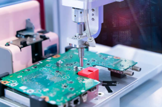
Surface Preparation: From this point in the process, the PCB boards are chemically and mechanically cleaned and if necessary, they are also subjected to various chemical treatments to promote adhesion of the plating material. It involves either electrochemical cleaning or manual removal with rocket abrasion.
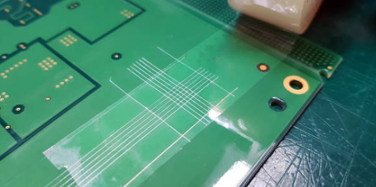
Electroless Plating: For some occasions, particularly with inner layer panels, it is possible that the board is subjected to the electroless plating process before the electroplating phase. In electronless picking, a very thin layer of conductive material is deposited on the inner hole walls by electrolysis. The material usually used as a coating is copper. This primary layer prepares for the application of subsequent electroplating, thus offering a conduit for electrical connection.
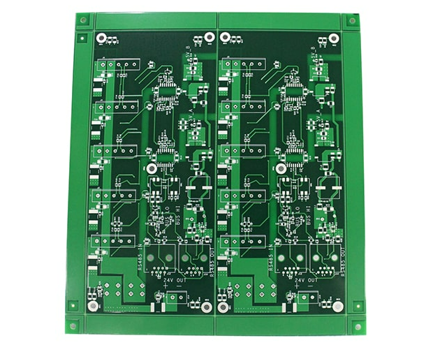
Electroplating: Electroplating is the main step of the plating method, where PCB panels are lowered and immersed in an electrolytic solution containing metal ions like copper ions. Under constant direct current (DC) conditions, the ions of metal in the solution pass through the layer and are left at the openings (holes) on the surface of the PCB. The metal ions go to the negatively charged plugin panels and form a thin film of metal via the electrodeposition process. This thin layer is reciprocally built up to the right thickness, which eventually creates a conductive route on the inside of the through-holes.
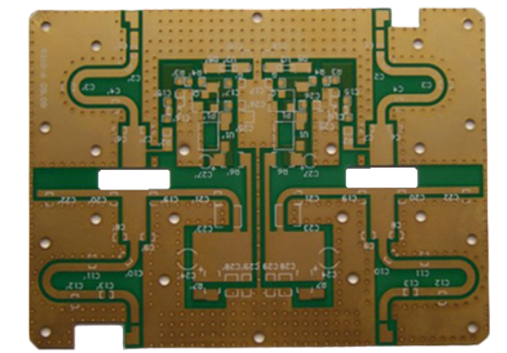
- Thickness Control: A controlled rate of epitaxial representative of the plated layer in electroplating is the basis of the electrical conductivity and mechanical strength of the vias. In this process, factors like deposition time, plate current density, temperature of the solution and the composition of the electrolyte are usually controlled.
- Post-Plating Processing: Following the electroplating process, the PCB panels may subsequently go through other steps of the process where the excess plated material will be removed, as well as other steps to ensure that the plated surfaces are smooth and that the plating across the PCB panel is uniform. Among these techniques, damping may involve chemical etching, mechanical polishing, or other surface finishing processes.
Quality Assurance: Plating and quality control measures are implemented during the plating process so that the vias meet the standards for conductivity, thickness, and adhesion to guarantee a reliable product. This may range from visual inspection, servicing of components, and other means of quality assurance.

In this way, the printed circuit board manufacturers use the electroplating technique to make vias with accurate dimensions, excellent electrical and thermal conductivity and reliable workmanship, a fundamental characteristic for the correct functioning of the printed circuit board in different electronic applications.
Types of PCB Plating
PCB plating is the process of applying a very thin layer of metal onto the surface of the board. This thin layer facilitates soldering and improves order performance and reliability. In PCB manufacturing, a variety of plating methods are utilized and every one of them has its own specific benefits and is therefore suitable for certain applications. Here are some common types of PCB plating:
Electroless Copper Plating:
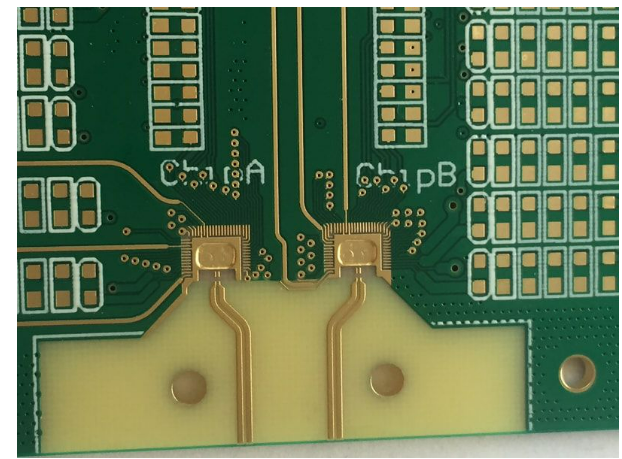
- Electroless deposition of copper film is a chemical process that does not need any external power source and can precisely place a thin layer of copper on the substrate of PCB. Otherwise known as electroless plating, it is commonly applied during PCB production as a first step to create an electrical conductive coating, which is later electroplated.
Electroplating:

- The most widespread method PVD, or anodization technology, for coating of vias, pads, and traces is electroplating. Metal icing is a process that implies embedding a PCB into an electrolyte solution containing metal ions, for example, copper ones. A current is then passed through the solution. It is the negative charge at the corroding PCB surface that immobilizes the metal ions as they are being deposited onto the exposed surfaces, and so a metal coating is being formed.
Immersion Plating:
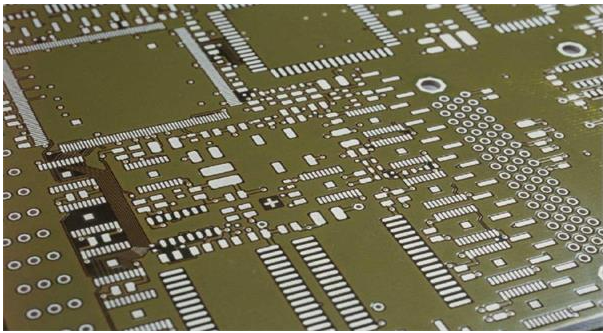
- Immersive plating, also known as chemical or displacement plating, refers to the technique of dipping the PCB in a solution of gold or tin ions. Atoms of the metal ions are captured and reduced to molecules that are packed on a PCB surface, forming a thin conductive metal layer. Plating by immersion is typically used for covering the copper surfaces which are unprotected, as it not only helps in retarding the oxidation process but also makes solder easier.
Electroless Nickel/Immersion Gold (ENIG):
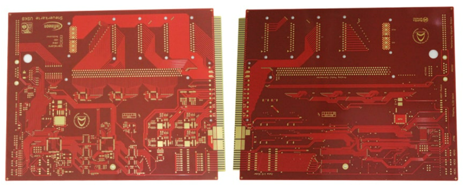
- ENEG surface finish is a common surface finish for PCB, especially when the intended applications require maximum reliability and solderability. The process starts with the deposition of electroless nickel of a small layer onto the unexposed copper tracks of the PCB. Then, the gold immersion comes in. ENIG offers outstanding corrosion resistance, soldering compatibility, and smoothness to enable wire bonding that is used in fine-pitch components.
Electroplated Nickel/Gold (Ni/Au):
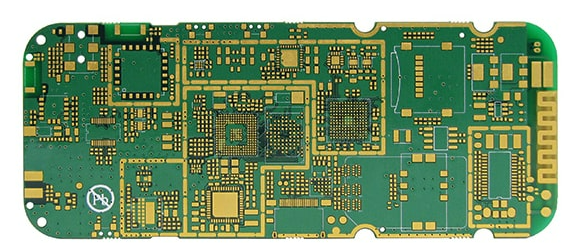
- Direct gold or nickel plating is an alternative surface finish for the PCB which is frequently used for applications that require higher level of protection against corrosion and wear. It includes a sequential deposition of the nickel by contact electroplating, followed by gold electroplating onto the copper lands of the PCB (Printed Circuit Board ). Nickel offers a barrier to oxidation as well as diffusion, and gold offers great conductivity and solderability.
Hot Air Solder Leveling (HASL):
- HASL is an old plating method that is usually employed for traditional surface finishing of PCBs, and this does-apply for both flat and through-hole components. This is done by melting a lot of solder on top of the PCB completely and then moving it down the throat of a hot air gun, ensuring that the extra melt is removed, leaving a thin, even coating of solder on the neighboring copper tracks. HASL achieves good solderability and is affordable, but it is ill-suited to expensive common shapes due to an irregular surface topography.
Organic Solderability Preservatives (OSP):
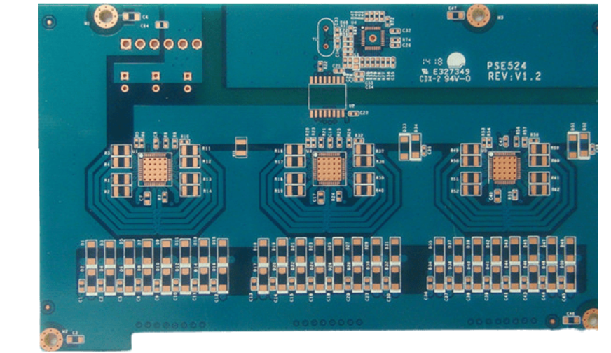
- The OSP is an organic thin film which is being used to cover the copper surfaces of the PCB in order to prevent oxidation occurring and to improve the reliability of the soldering process. SMT is regarded as the primary application of OSP, where flatness, fine pitch, and a surface with no defects are of utmost importance. It is a rostrum for printing or spreading solder paste, implying that it is friendly to silver-containing soldering processes.
These are the most common types of copper/tin alloy layer pcbs used in the industry, all remarkable for their distinctive properties and advantages related applications. The plating method would be decided based on a number of factors, including what properties should be attained, the economic aspect standard plating, and overall compatibility of the chemical process with the assembly processes.
Copper Plating Process During PCB Fabrication
A copper plating process is an indispensable element during the fabrication of printed circuit boards, and this one assists in creating properly-conducting electric lines from the components to the traces. It typically starts with surface preparation as a precondition to get rid of dirt and treat the surface for the adhesive. Overall, surface preparation is an indispensable part of a successful paint job that brings aesthetics and durability to residential buildings. Then, precision drilling machines puncture the holes at specified points where vias and component mounting pad are mounted. With the use of electroless copper deposition on the vias that are already drilled, the following electroplating process can be carried out and the desired electrical connections between the layers of the PCB circuit can be established. The subsequent plating operation done by immersion in an ion-containing Cu electrolyte solution happens thereafter. Utilizing an electric current injected into the solution materials would result in copper ions being attracted to the surfaces and, subsequently, a more uniform and thicker layer of copper deposited. The servo plating process guarantees complete copper layer surface coverage, which in turn secures sufficient conductivity evenly across the PCB.
PCB Plating Process for Applying Surface Finishes
The PCB plating process is considered to be the most critical one during subsequent stages and is required for maintenance of the printed circuit boards’ integrity and functionality. It typically starts with surface preparation, where PCB substrate is treated and cleaned to carry out the removal of contaminants and ensure a good bond. Subsequently, such as pickling, various surface finish methods are carried to form a barrier against the exposed metal and provide the required electrical properties. Using gold electroplating is one of the typical techniques, usually ENIG (nickel immersion gold), which is characterized by a two-layer process (the application of a thin first layer of electroless nickel and immersion into a gold solution). This is why this process guarantees top corrosion resistance, solderability, and flatness varieties, ideal in fine-pitch components and wire bonding. The next widespread surface finish is hot air solder leveling (HASL) People usually use leveling, which implies that the entire board is coated with molten solder, which ensures good solderability and protection from oxidation. HASL is a popular wave solder process that is for through-hole assembly mounting subcomponents, but it may not be applicable if fine-pitch parts of the PCB interfere with the surface topography. Furthermore, organic solderability preservatives (OSP), which act as an anti-oxidant to prevent copper surfaces from oxidation, improve solderability in application where surface mount technology (SMT) is used. OSP refers to a uniform surface, thereby enabling the solder paste to be evenly applied, and it is compatible with lead-free soldering processes. The used surface finishing methods in manufacturing PCBs are essential if the quality and performance of the PCBs in the electronic sphere are to be put to the test.
Barrel Cracks
Crack barrel is a term that indicates vulnerability of the PTH on a printed circuit board (PCB) where it fails at the break point during PCB manufacturing due to the thinning of copper plating used. The requested sentence implies that these corrosion cracks can weaken the structural integrity of that electrical connection, that leads to unreliable performance of the PCB. There are several potential causes of barrel cracks, including:
- Overetching: Over etching in the PCB-making process often leads to thinner walls of the barrel, which might result in a crack along the barrel length. Underetching may sometimes occur if the process control is not maintained properly or after exposure to the chemicals used in etching for long time.
- Thermal Stress: The thermal stress during the process of soldering and reflow can lead to expansion as well contraction in the printed circuit board substrate and the plating in the interconnections. This process may generate stress on the barrel and visible cracks, which becomes more evident over time.
- Mechanical Stress: The mechanical stress which has been related to the handling, assembly, or operation of the board can also cause a barrel crack. Too much stress put on the board during the handling or pushover can cause micro-deformations or fractures to begin in the through-hole barrels. They can then sprout and stretch into the whole layers.
- Plating Defects: Inadequate plating coverage or voids within the barrel can create weak points that are susceptible to cracking. Plating defects may result from process variations, contamination, or improper plating conditions.
- Material Incompatibility: If the variables of materials and plating procedures are not matched or if the coatings show different rates of thermal expansion or contraction, contact points will be created and stress concentrations will take place, eventually leading to cracking.
- Environmental Factors: Exposure to a range of harsh environmental conditions, such as high humidity, temperature extremes, or chemical contamination, increases degeneration of PCB structural materials and encourages barrel cracks formation.
In order to avoid barrel cracks, they highlight the need to apply the best practices adopted in PCB design manufacturing, and assembly. This type of process optimization will involve etching process optimization, temperature control during soldering, complete plating assurance, material compatibility and use of verified assurance control measures throughout the PCB production process. Moreover, the correct storing abilities and handling practices can prevent the infrastructural damage and environmental degradation of barrel fatigue.
Conclusion
In conclusion, the plating thickness is of extreme importance in terms of the reliability, conductivity and mechanical strength of printed circuit boards. How thick the plating layers involves an important factor for firm and strong electric connections between different layers of the PCB, particularly in high-density design with fine-pitched components. Thick plate height sufficiently improves the mechanical strength of vias, which manifests in reduced incidence of solder joint fracture or barrel cracks. Furthermore, uniform plating thickness should not be overlooked since continuous signal integrity and impedance control, especially in high-speed RF, are the factors to be considered. Nevertheless, the thick plating and excessive plating can cause some problems, like nosing calibre drops, increased cost and production problems. Therefore, the correct balance of plating thicknesses is of crucial importance; the designers, manufacturers and reliability specialists should carefully understand the requirements and opportunities of the technology. Overcoming this challenge by means of plating thickness calibration must be made in order to meet the exact PCB reliability and performance needs whilst using minimally disrupted production processes.

