PCB’s are the spines of modern electronics, they power everything from the tiniest sensor to a considerable computing center either power and ground planes. In the history, they turned out to be the most outstanding and industrious catalysts, which changed the way we use, create and manufacture all electronic devices. In this blog, we’ll have a look through the height range of PCB applications to show their multi-functionality as well as the decisive part of the various industries.
What is a printed circuit board?
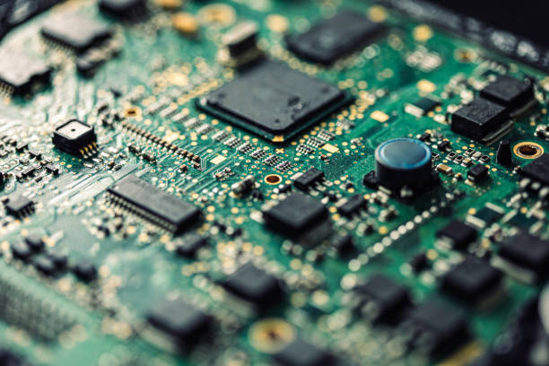
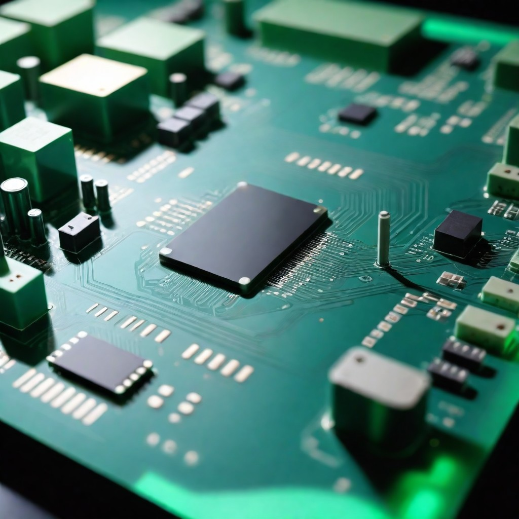
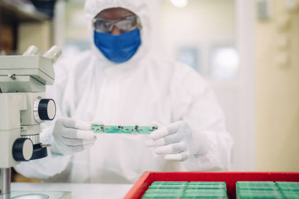
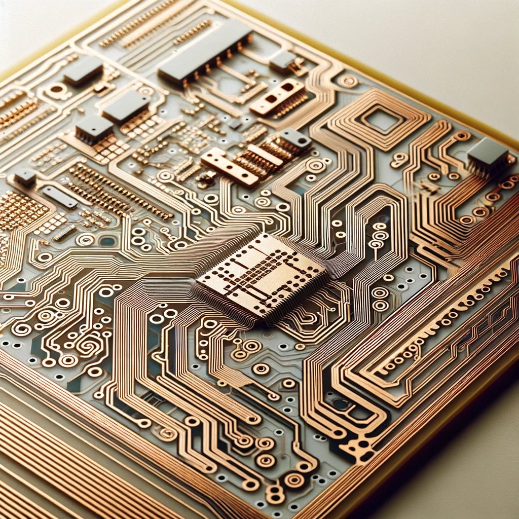
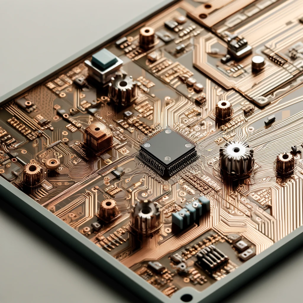
A printed circuit board (PCB) which stands for a physically backed electronic component placement supporting pad and another feature with conduction pathway using a copper laminated sheet as a substrate.
The basic structure of a PCB
The basic structure of a PCB typically includes the following:
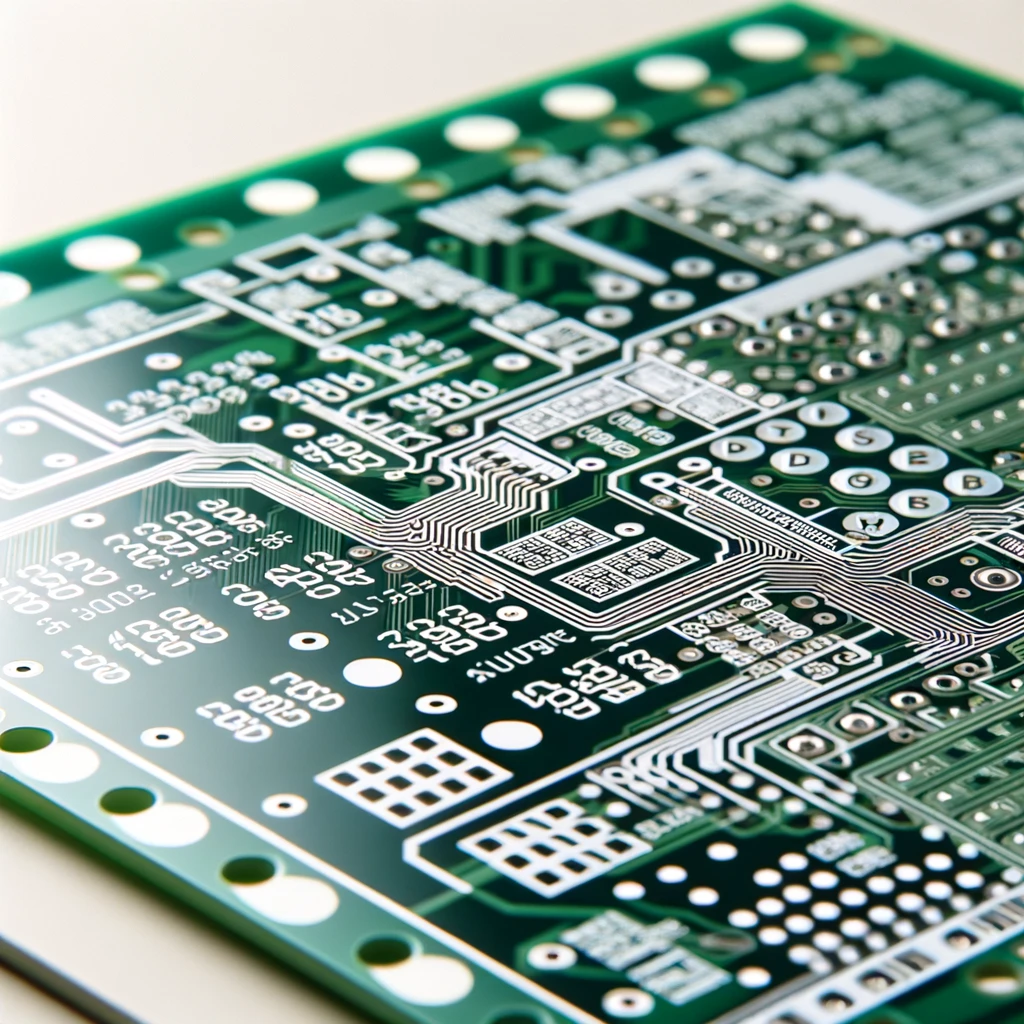
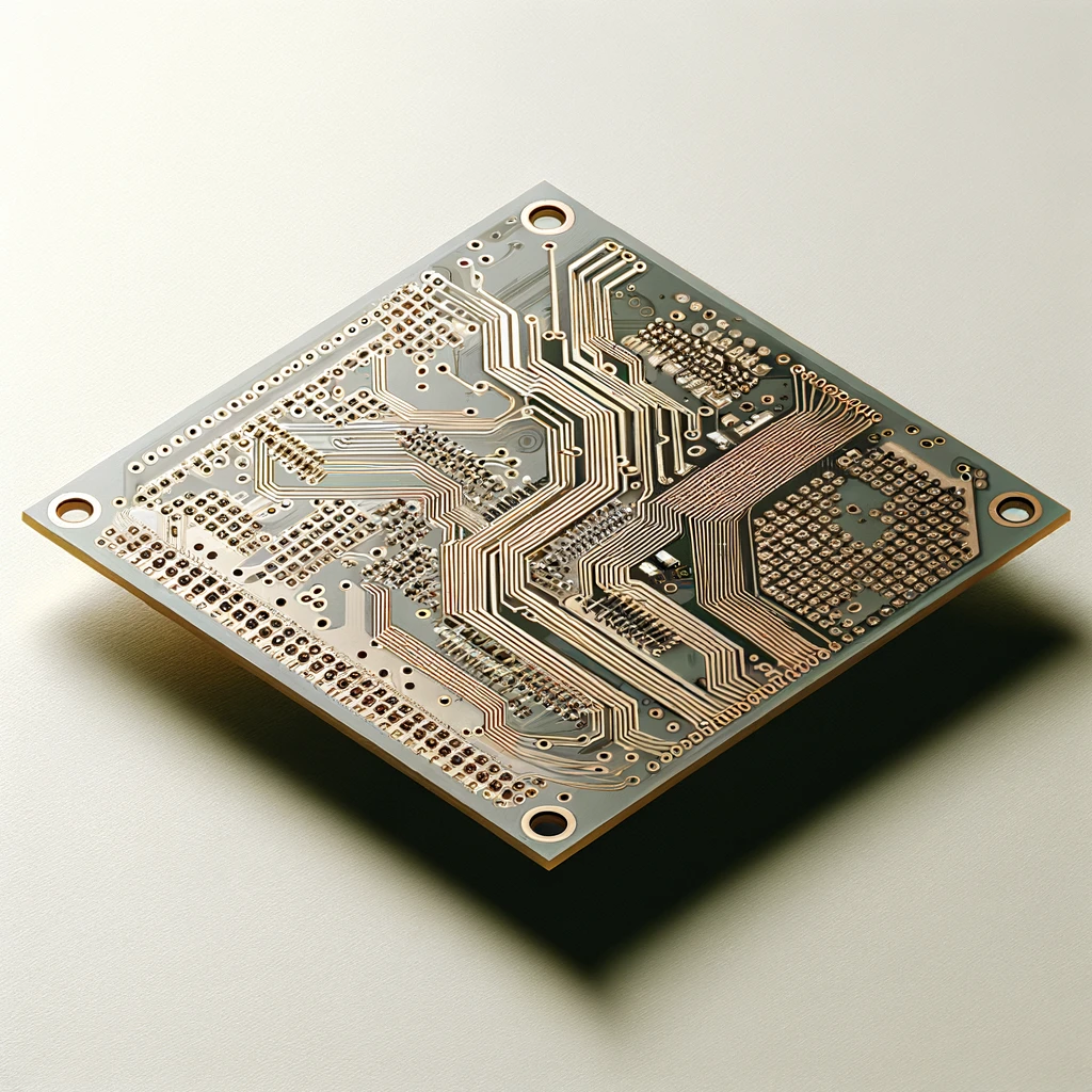
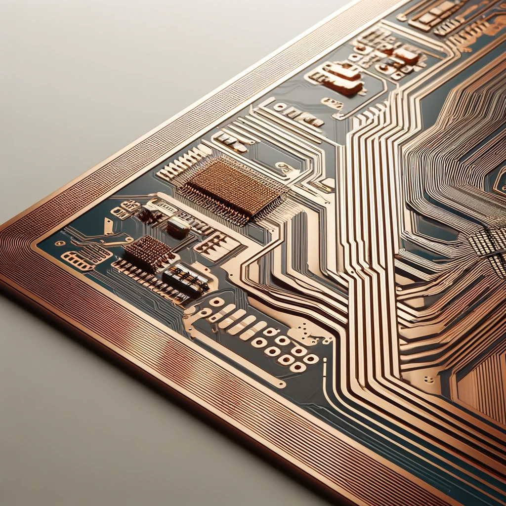
Substrate: The table Fabric the Flat PCB is usually made up of Fiberglass, like FR4, which provides it with the characteristics of flexibility and strength.
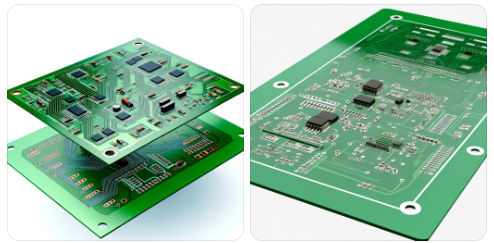
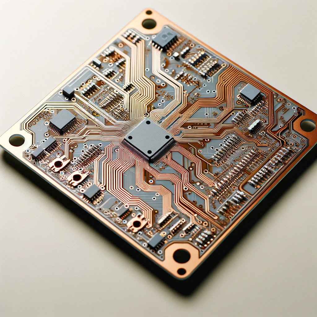
Copper Layer: This can be seen on either or both the top (or the bottom, depending on the type of PCB) where the actual device is connected to circular pads. The copper is initially poured in all the board areas and then removed to the places that are not in need, hence keeping only conductors (lines of copper) that link thereof PCB.
Solder Mask:Above the copper layer, one can find the silkscreen layer which is usually green but may come in other colors (red, blue, and such). This layer also act as insulator, so the copper traces cannot exhibit oxidative behavior with other metals, solder or conductive.
Silkscreen: Moreover, addition white ink (i.e. silkscreen print) can be utilize to write component values, labels and other symbols as well as anything that would help in installation or circuit understanding.
What are PCBs used for?
Printed circuit boards (PCBs) have multiple applications: among the devices that incorporate these boards, the most important aspect is to provide a stable platform when connecting all the electronic component. In doing so, they operate all these units through generators featuring electrical conductors. Here are some primary uses of PCBs so circuit boards are used:
- Consumer Electronics: Products in the categories such as smartphones, computers, TVs, and home appliances.
- Medical Equipment: When implanted in the person, these devices can precisely and reliably work in the area with a constant DC field in the pacemakers, MRI scanners or blood glucose monitors.
- Automotive Components: In the modern vehicles just like modern printed circuit boards it is the systems like: engine management, entertainment, and driver’s cabinet among others, that makes everything so easy and makes driving so pleasurable.
- Industrial Machinery: In this regulatory context, IoT is particularly relevant for control systems of manufacturing equipment, robots, and assembly lines.
- Telecommunications: equipment like routers, switches, or base stations which make sure that the data is transmitted well.
- Aerospace and Defense: For instance, in aircraft, satellites, and defense systems where durability and reliability are success key factor, electricity is the main enabler.
- Wearable Technology: With smartwatches, fitness trackers, and other similar gadgets, we can quickly view whether we are ready to complete our daily exercise requirements or make healthy food choices.
- Internet of Things (IoT): smart home appliances, environment monitors, and several taken-for-granted connected devices which form the basis of the Internet of Things(IoT).
What are pcb used for? PCBs give a completely new meaning to the technological and industrial sectors by allowing the creating of multi-layered super thin boards which enable supplying of electrical signals and power to capacitors and symbiosis between dispersed electronic components.
What are the different types of printed circuit boards, and what are they used for?
This term, PCBs of different kinds is provided for specific functions within environmental conditions such as position and operating conditions of internal devices. Here are some of the main types of PCBs and their typical uses like almost every electronic device:
Single-Sided PCBs
The manufacturer applies the upper and lower conductive layer, usually represented by copper, to either one side of the surface mount the insulator substrate. One side is for components, the other one metal etching makes circuit.
- Use: Besides radios, computers, and surveillance cameras, these categories contain the most affordable and basic electronic appliances like radios, calculators, and other consumer goods.
Double-Sided PCBs
These copper layers are essentially like the veins on the surface top and bottom layers of the substrate. Peices can be put on the left or right side, whereas circuits can traverse on one side via hole(s).
- Use: Able to be adopted in applications that are driven by medium complexity, such as power supplies, industrial control systems, car dashboard and light emitting diodes (LED).
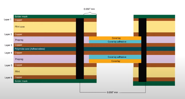
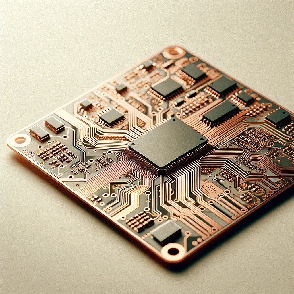
Multilayer PCBs
The variety of PCBs which can be designed is broad from standard, single sided boards to two-layer single circuit boards to complex triple-sided boards that are wire-wrapped together. They are insulated by the fluoropolymers or SiO2 materials and with vias to connect them. Mulitlayer PCBs can have up to 4 layers but also can have more than 30 layers.
- Use: These are working in integrated and overlapped devices that require several component levels, such as computers, smartphones and advanced healthcare and defense systems.
Rigid PCBs
Fiberglass used as the core that gives the substantial, rigid surface or rigid substrate to provide the board has no flexibility. Renewable low carbon carbon footprint materials such as recycled metals are the most used types as electronic products used small consumer devices today.
- Use: His invention has led to the development of flexible, bendable, and rollable screens, which are changing the landscape of electronics ranging from computers to TVs, and household appliances.
Flexible PCBs
The use of flexible substrates like polyimide demonstrates knowing how to mold. These flexible printed circuits boards can bend and twitch that opens the door just like modern electronic door locks to be used where rigid printed circuit boards cannot fit in, for example, smartphones and wearable devices.
- Use: Exemplification of continuous solder interconnection application where reliability is key, e.g., smartphones, wearable sensors and devices like the foldable ones or compact electronic device.
Rigid-Flex PCBs
These have constituent parts of the printed circuit board assembly as both of them are flexible and hard materials. They are popular in the manufacturing of parts of panels which often involve such areas that bend during use while the remaining others stay constantly rigid.
- Use: Utilized in advanced electronics such as parts of the PCB that need to be flexible while others have to remain rigid; Gives you examples of where it is used a lot: like the aerospace, military, and the complex consumer electronics.
High-Frequency PCBs
Designed to oscillate in the high frequency ranges. The PCB is made of the laminated materials that support high-speed signal performance without noticeable loss; Rogers and Teflon are the commonly used ones.
- Use: The machinery is built for high speed and high frequency applications, e.g. telecommunications equipment, microwave technology and RF apparatus.
Aluminum-backed PCBs
These ones are made of metal, usually aluminum; the metal explains why their job is to absorb heat. They are usually found in for high-power applications like LED lighting, wherein the temperature control is of utmost importance.
- Use: Perfect fit for applications that produce considerable amounts of heat and correspondingly require good heat dissipation, like light emitting dioded ones and power supply units.
HDI (High Density Interconnect) PCBs
Include a wiring density that is two-fold times more compared to traditional PCBs area-wise. HDI PCBs are fashioned by smaller features, rows and spaces, narrower vias, thinner pads, and dense connections.
- Uses: smartphones, matic, security cameras, wearable technology, medical devices, automotive electronic composition, aerospace components and components for IoT devices. Manufacturing process for printed circuit boards requires multiple steps
Step-by-Step
1. Design and Layout
The process goes on by way of complex process of carrying out the design of the PCB through the software titled CAD. Engineers produce circuitry layout, describing the position of components (e.g. resistors, capacitors, etc.), electrical paths, and any other features that must be availed.
2. Printing the Design
A pattern of the design, which will be printed on a specialty film, will be used to transfer the pattern onto substrate made of copper-plated material. It is particular PCB that displays where exactly the copper traces are supposed to be on the actual printed circuit board.
3. Preparing the Substrate
Generally, the manufacture circuit card assembly of a PCB is made on a non-metallic substrate of glass fiber, often referred to as FR4, with a thin layer or multiple layers or internal layers of the copper material on one or both sides. A layer becomes coated with a film that is then etched to form the circuit pattern.
4. Transfer of Circuit Image
The printed film circuit based design is transferred onto the prepared substrate during a light sensitive/photological method called photolithography. This kind of work involves the covering of the substrate in photomasking material that is imaged with UV light, then allowing the light to come through the image. By exposure to the air, the material becomes solid in these areas, but in other areas, where the material is covered, it remains pasty and is then removed.
5. Etching
The photoresist is then the hardened with chemical etching which removes the raised copper and leaves the top of the copper traces where the hardened photoresist was masked.
6. Drilling
Holes are tapped out in PCB which is for surface mounting the components and Vias which are for connection of different layers of a multilayer PCB. This may be done either by a directly controlled computerized drilling machine or by using hand tools for follow-up drilling.
7. Plating and Additional Copper
The hole is done after which the board now proceeds to the plating process where through hole components it is struck with more copper deposit that in turn provides the plated-through vias, connecting the different layers of the PCB.
8. Application of Solder Mask
The entirety of the existing PCB is covered with a solder mask material apart from soldered contacts layer. This mask avoids the lucky strike, bridging caused by solder jumping to neighboring places.
9. Screen Printing
Direct printing of labels and legends with silkscreen is one of the graphics methods used to provide instructions of assembly and component locations to aid assembly in this manufacturing process.
10. Surface Finish
A LED surface finish is specially designed to provide mechanical support for the copper pads in establishing an antioxidant coating and therefore help solder during component assembling.
11. Testing and Quality Control
The finished assembly will run all electrical checkouts with the purpose of attaining capabilities and specifications as per requirements. The task of this kind might be divided in parts: continuity and isolation tests to determine whether the connections and the disconnections of the intermediated circuits are proper, respectively.
12. Cutting and Profiling
Using a cutter, the particular PCBs are now separately cut apart from the larger panel that many PCBs were simultaneously fabricated. Routing ways can either be done using routing machines or laser cutters.
13. Assembly
For most PCB making and assembly processes, however, the final stage is preparing the components to mount on the circuit board, which brings the PCB to full functionality. This requires assembly of components and their soldering on the board leveraging automated pick-and-place machines and reflow soldering methods.
Where can I get printed circuit boards?
Different from the case of printed circuit boards (PCBs), these are procured from the specialized manufacturers/companies only. These are locally and internationally accessible as well, as many companies have PCB custom production services that are already offered online. Similarly, electronic hobbyists can buy PCBs for their projects from electronic component stores or online shops like Digi-Key, Mouser Electronics, and Alibaba.
How do printed circuit boards get into the environment?
The printed circuits boards may find ways to enter the environment at different shipping routes, but mostly at the end of their lifecycle. Here are the key pathways:
- Electronic Waste: If electronic devices are not discarded properly, obviously printed circuit boards (PCBs) inside them will contribute to the total electronic wastes (e-waste). On the one hand, this accumulative waste could finally be disposed of at landfills if it is not recycled properly.
- Landfills: In landfills, PCBs can decompose over time, hidden substances like lead and mercury and cadmium being released afterwards to the soil and the groundwater.
- Incineration: If e-waste having or PCBs is disposed in an incinerator which is not equipped with veriable controls, toxic materials may be released into atmospheric air, which indicates that emissions of health-threatening and environment-contaminating substances may occur.
- Improper Recycling: Without correctly implemented PCB processing systems, these pollutants can be released through accidental of negligence (not) disposal.
Effective recycling and remanufacturing are vital in mitigating PCBs pollution, especially through, when emphasis is on good electronics recycling practices.
How can printed circuit boards affect health?
Printed circuit boards (PCBs) posses a health risk by being exposed to toxic compounds which are used in their production or are released during their recycling, manufacturing processes, or disposal. Here are the primary ways PCBs can impact health:
- Heavy Metals: Generally, PCBs containing mercury, lead, and cadmium heavy metals. The occurrence of these substances can be possible when, during PCB’s improper handling, disposal or recycling, they are either intentionally or unintentionally released into the environment. It is a source of numerous health problems such as neurological, kidney failure, and other organs while conditions.
- Chemical Exposure: While manufacturing and recycling PCBs, hazardous chemicals like brominated flame retardants may escape into the environment to oxidize and start the fire. Such a massive range of chemicals are suspected cause of endocrine disruption, developmental problems, and other chronic diseases.
- Airborne Pollutants: When PCBs do not receive appropriate incineration, dioxins and furans can be released into the environment. These are extremely toxic chemical and may remain in the habitat for a long time. This take of these pollutants can be inhaled to respiratory problems, cancer and other serious health conditions.
- Water and Soil Contamination: The act of leaching of poisons from a landlike PCBs can pollute fresh water and soils of a given area. This contamination not only can concerned with the human health but also with wildlife, possums, the food chain could be polluted over time.
- Direct Contact: Workers in the industries that are connected with manufacture, disposal, or recycling of PCB might be exposed to direct skin with the dangerous stuff, which may induce skin irritation (redness or rashes), allergic reaction or acute dermatitis.
Health risks can be reduced by compliance with safety standards while fabrication, movement, and disposal of waste are held to the highest standards to bare board. It is also crucial that efficient recycling approaches are in place to prevent the release of harmful substances into the surroundings
Industrial equipment: wise application of PCBs
Printed circuit boards (PCBs) and printed wiring board and etched wiring board play a fundamental role in industry and its production facilities, acting as the backbone for maintaining integrity and coordination everywhere, regulating operations, security systems, monitoring systems, and ensuring reliability and efficiency. Here’s how PCBs are wisely applied in industrial settings:
- Automation and Control Systems: PCBs are the main parts on PLCs and other automation equipment, since they help to maintain a fine control over machine movement and industrial processes.
- Industrial Robotics: Applied in the portion of hardware of the robots’ systems which include electronics interfaces, sensor integration, and motion control, the PCBs aid in complex operations in automation and production.
- Power Equipment: PCBs are essential components in power generation and distribution circuits, that mainly are equipments of the converters, inverters and UPS systems designed to handle more power and heat loads.
- Monitoring and Diagnostic Systems: In sensors and diagnostic tools, PCBs detect continual industrial indicators such as temperature and pressure, helping minimise downtime by enabling predictive and preventive (predictive) maintenance and system efficiencies.
- Communication Devices: The first task of any PCB in a complex industrial communication system like transceivers and signal boosters is to ensure the stability of the data transmission across facilities; Therefore, the PCBs are designed in a way that they make the data transmission reliable.
- HVAC Systems: PCBs monitor, control and regulates the heating, ventilation, and air conditioning systems, keeping the best environments not only for the products, but the personnel as well.
- Safety and Security devices Equipment: At the critical point of safety systems alarms and emergency close down, PCBs ensure safe and dependable operation even under severe conditions.
- Testing and Measurement Equipment: PCBs are integral components of provisional testers deployed in manufacturing to ensure product quality and process monitoring, which enhances product consistency.
- Manufacturing Equipment: They ensure manufacturing process by CNC machines, which is the more skilled operation than workers, enhancing productivity and precision of the line of production.
The case of the Schneider generators unveils the fact that PCBs are essential for the smooth, reliable, and safe operation of these generators and probably of many other pieces of industrial equipment and also medical imaging systems.
FAQs
Here are some frequently asked questions (FAQs) about the use of printed circuit boards (PCBs):
- What are PCBs used for, in general? PCBs are comprised of non-conductive substrates onto which a conductive copper sheet is printed and laminated to form the solder pads, vias, trace layers, or inner copper layers and other components used to support and electrically connect electronic components through conductive pathways, tracks, or signal traces. Electrolytes are used in building modern electronic devices because they are essential components of the same.
- In which consumer products are PCBs most commonly found? PCBs can be found in almost all sorts of electronics used by the consumer including continental phones, computers, televisions, radios and many others.
- How are PCBs used in the automotive industry? Similarly, in the automotive domain, PCBs are implied in the control systems, entertainment systems, navigation systems, and also, the safety features like airbag systems and anti-lock braking systems.
- What role do PCBs play in industrial applications? PCBs are a crucial tool for automation in industrial environments, power systems, robotics systems, and process controllers, among other things, to the betterment of their working time and functionality.
- Can PCBs be found in medical devices? Yes, indeed, PCBs are used in the availability of medical devices which are portable and are used, e.g, as monitor screens, imaging tools like MRI machines and moreover implantable devices like pacemakers.
- How are PCBs utilized in telecommunications? As for modern telecommunications, PCBs are not dispensable; they play a critical role in the equipment performance enabling the process of data transmission and signaling in devices like routers, switches, and base stations.
- What is the importance of PCBs in modern computing? PBCs are core elements in all parts of computing environment: those every day computing from home and office workstations to the highly complex and integrated data centers and servers, used by many Internet service providers, which are the more powerful versions of their desktop computers.
- Do PCBs have applications in aerospace and defense? PCB boards in the aerospace and defense industries are used due to their reliability and immunity to extreme conditions. Aircraft communications or avionics as well as military hardware do need these boards, the main ones, to operate properly.
- How do PCBs support the development of wearable technology? With the help of PCBs, other electronic components that comprise wearable technology can be miniaturized. This is in favor of features that include wireless communication, sensor integration and small-scale power management.
Conclusion
Along with multiple functions, the flexibility of PCBs is key drivers of innovations in all technological and industrial disciplines. You may think of them as only workhorse wires in their process of carrying of electricity through the circuits, but they serve as the very foundation for the development in electronics. Along with technology advancement, the use of PCBs broadens bringing them to a vital and unique part of the digital world.
With the recognition of the many diverse applications of PCBs, we can see the embedded elegance and ingeniousness which most of us would never notice in the now ordinary gadgets and appliances in our daily lives that run on PCBs, which have become now ordinary.