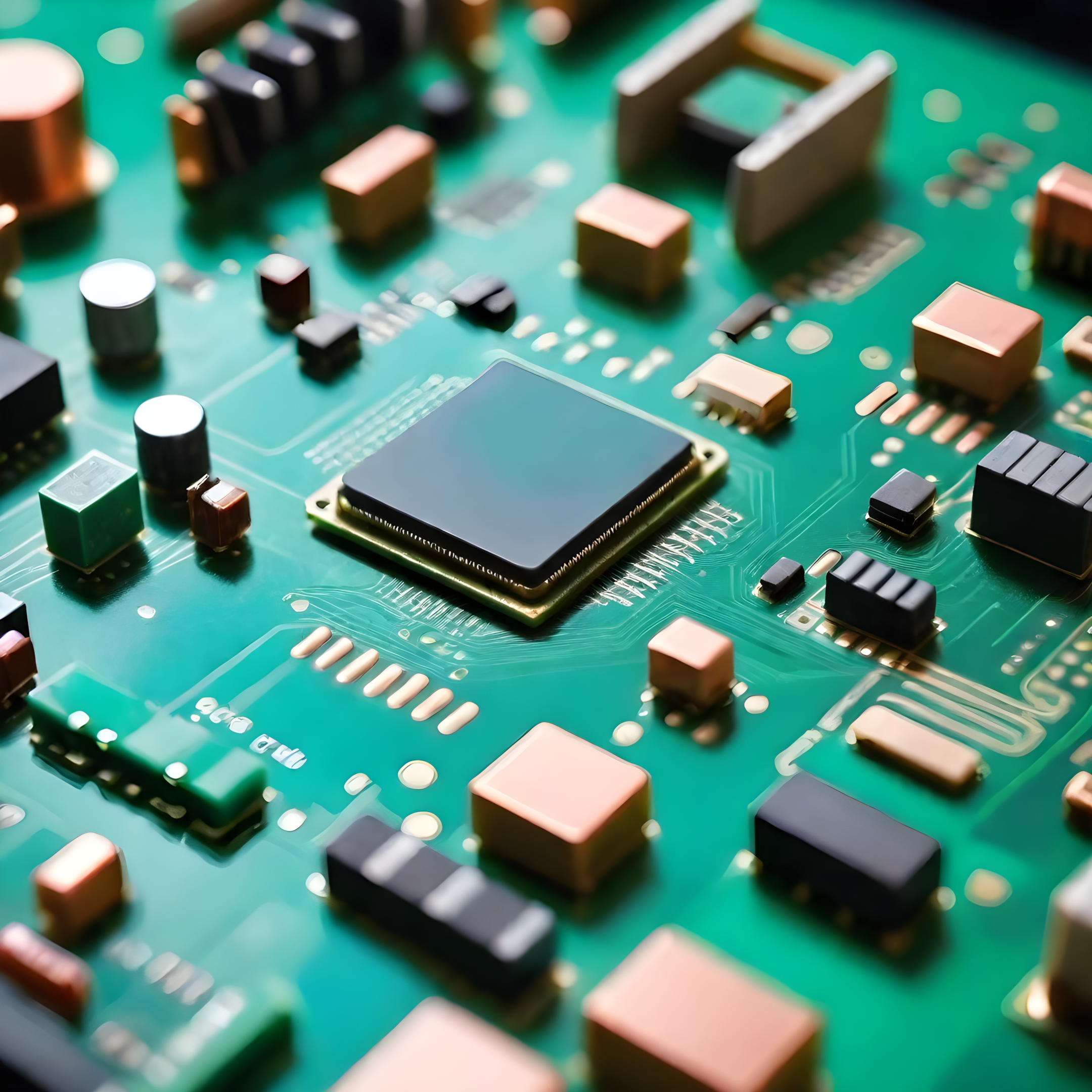
Printed Circuit Boards (PCBs) can be considered a ‘life-sustaining’ component of every electronic device, taking on the precise and reliable responsibility of supporting and interconnecting the electronic components. Prototyping and circuit board manufacturing begin with these simple PCB boards, which act as the foundation to build up complex circuits. In our step-by-step guide, we uncover the essence ofthe price of blank PCB boards, highlighting the various types, their use, and the prospect of limitless options as you create electronics designs.
What is a blank-printed circuit board?
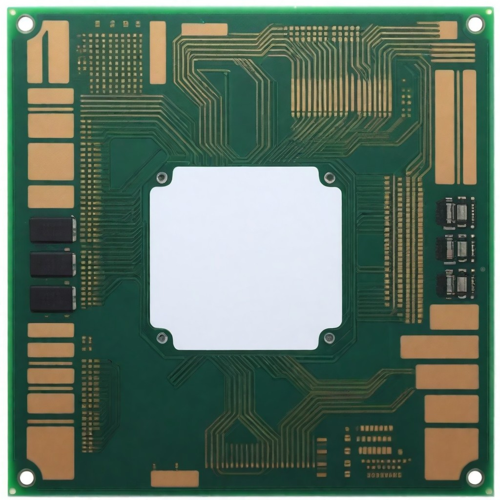
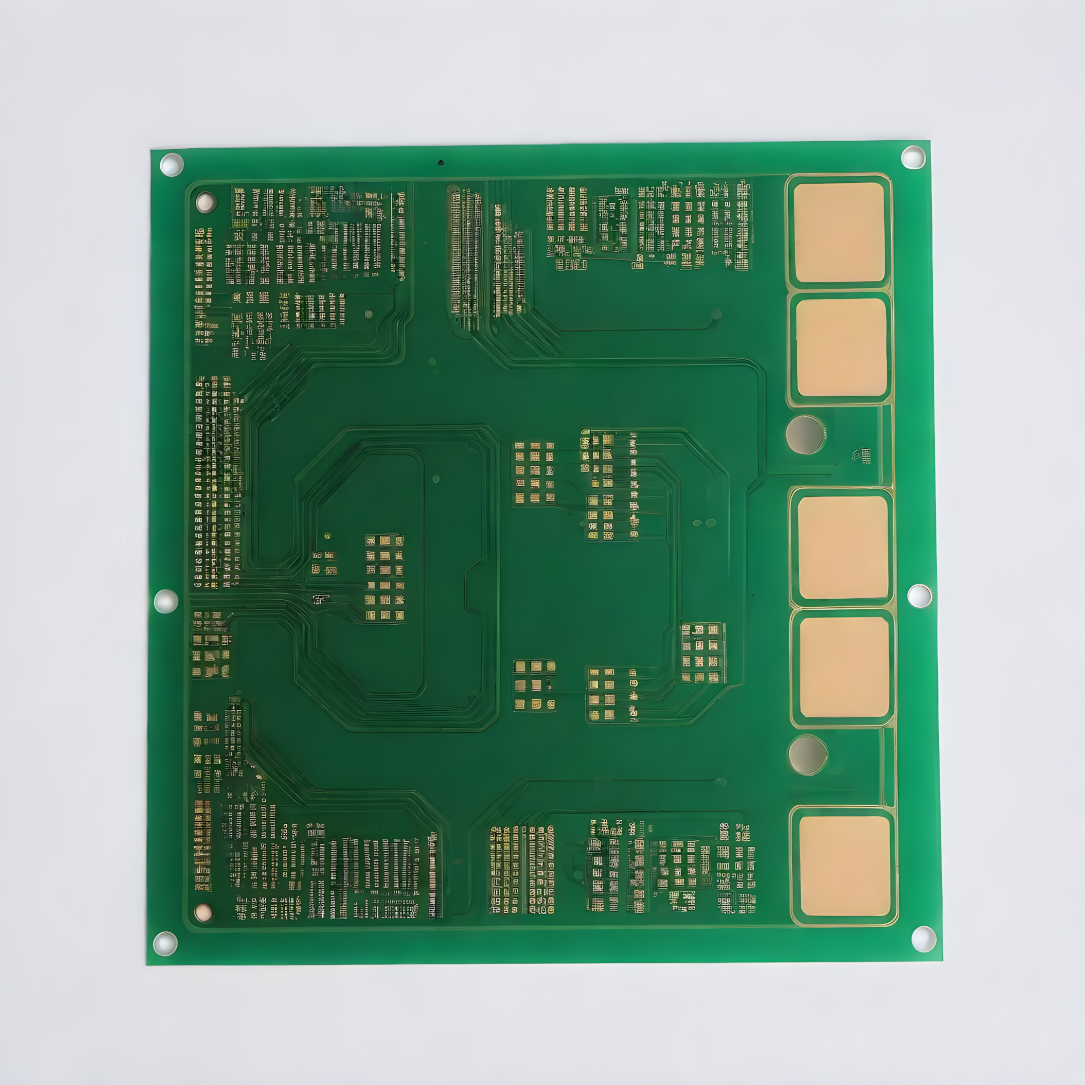
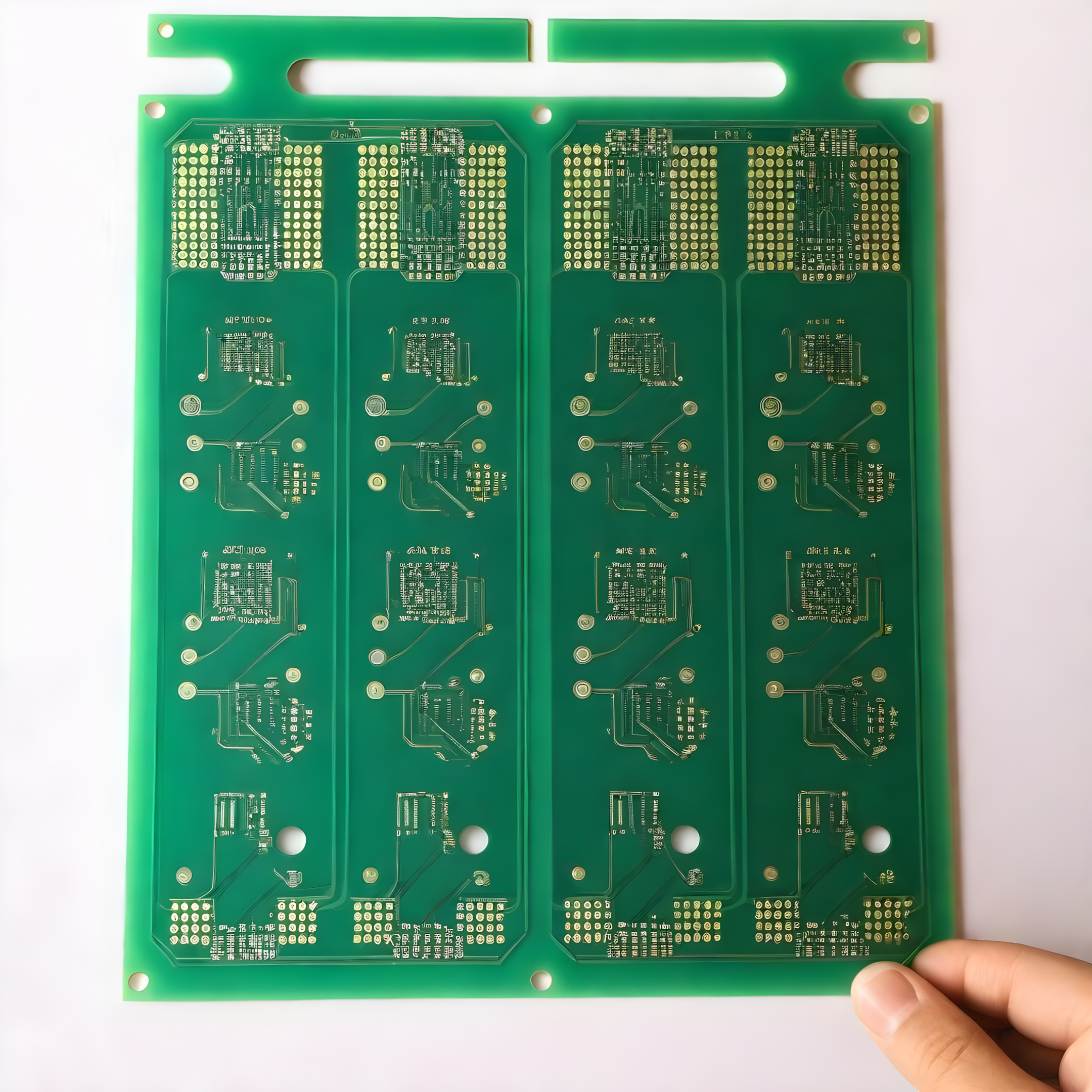
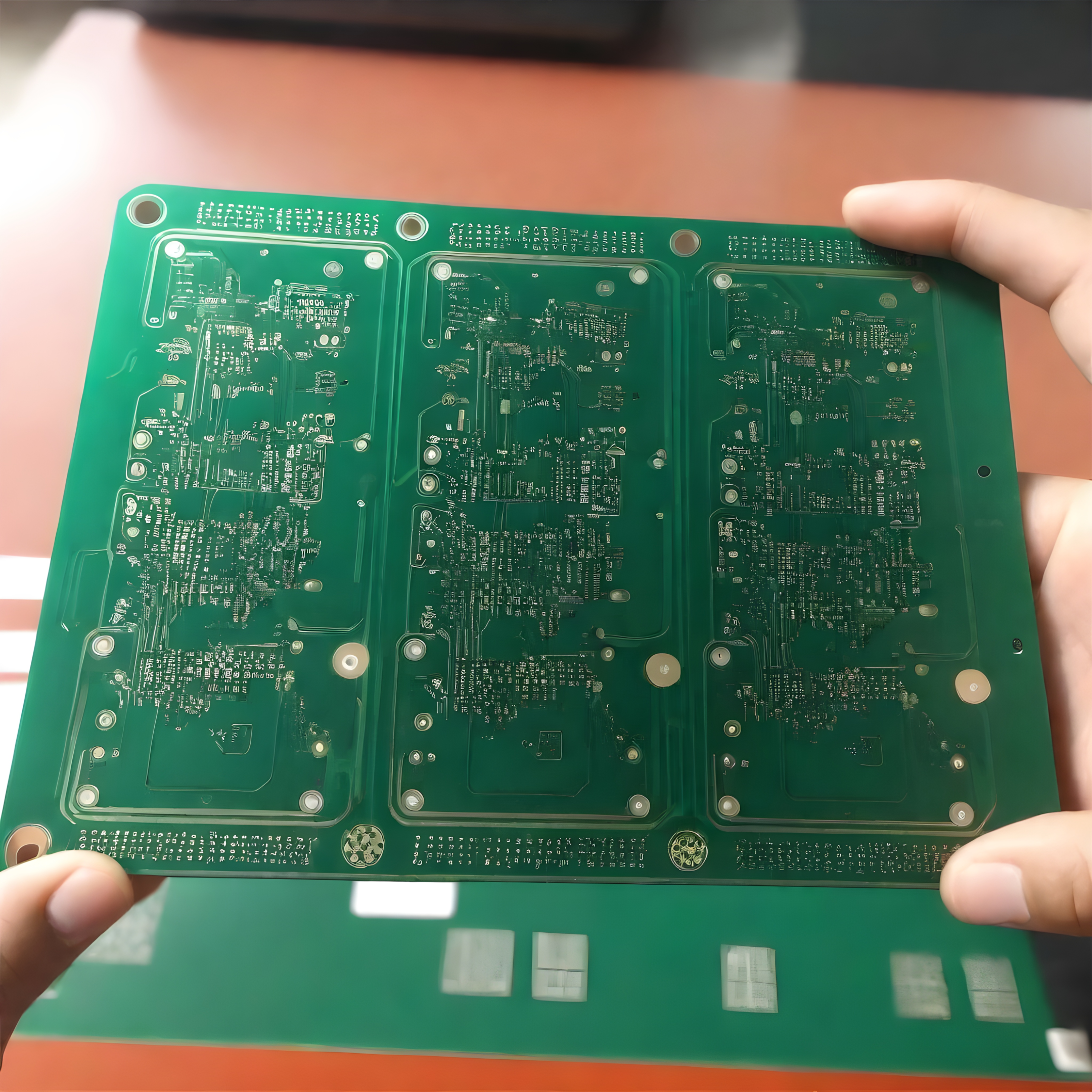
A bare or unpopulated PCB panel consists of multiple layers of copper laminated between non-conductive sheets. These blank boards are set as the beginning of the circuit board manufacturing line, which can be realized into practical PCBs by adding the electronic component and the conductive paths.
Types of Blank PCB Boards
Blank PCB boards come in various types, each suited to different applications and requirements: The PCB (Printed Circuit Board) boards are the primary connecting components in the electronics industry, providing the structure for mounting as well as arranging many components in relation to each other. Here are some of the main types of blank PCB board price you might encounter in 2024, along with the latest advancements or features:
Single-Sided PCBs
This type of structure is referred to as the simplest and is composed of one layer of conductive material, for example, copper traces, applied on one surface of the board divider, which is insulating. The opposite side of the components is the space for the circuitry, which in our design is printed on copper etching. They are very common in low-grade electricity use, such as in power supplies and in sensors.
Double-Sided PCBs
These boards have circuits on both sides, and they are connected through pin header holes. Thus, accessing from the back side becomes easier. These boards are suitable to be used for more complicated electronic devices than one-sided PCB manufacturers. The road ahead comes with additional achievements, such as updates in the way metal is processed to enhance connectivity and reliability.
Multilayer PCBs
Constructed as multi-layer boards composed of 3 or more layers of fiberglass-resin prepreg separated by high-thermal-conductivity insulation material and bonded at elevated temperatures, multilayer printed circuits are a key solution to facilitate the line of high-speed circuits. Nowadays, fashion is going to layer the amount with more function while reducing the total thickness of device to improve the signal quality and require advanced materials and also diy multilayer pcb.
Flexible PCBs (Flex PCBs)
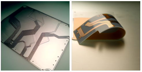
Consisting of materials that can be bent more and flex, these are especially used in compact applications or dynamic devices like wearable devices. However, the innovation that takes place in 2024 will pay greater attention to long-term sustainability and integrate more capabilities into even smaller footprints.
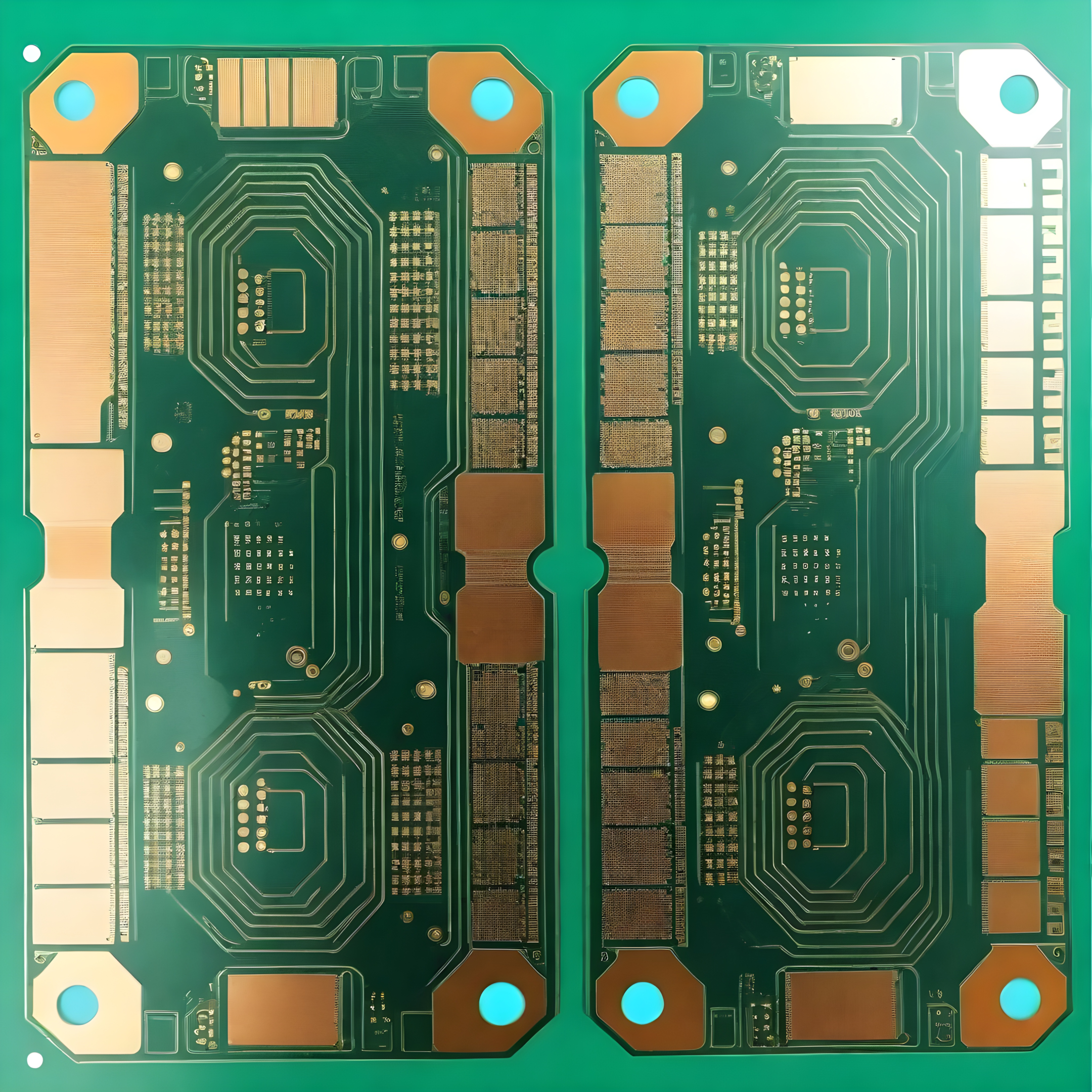
Rigid-Flex PCBs
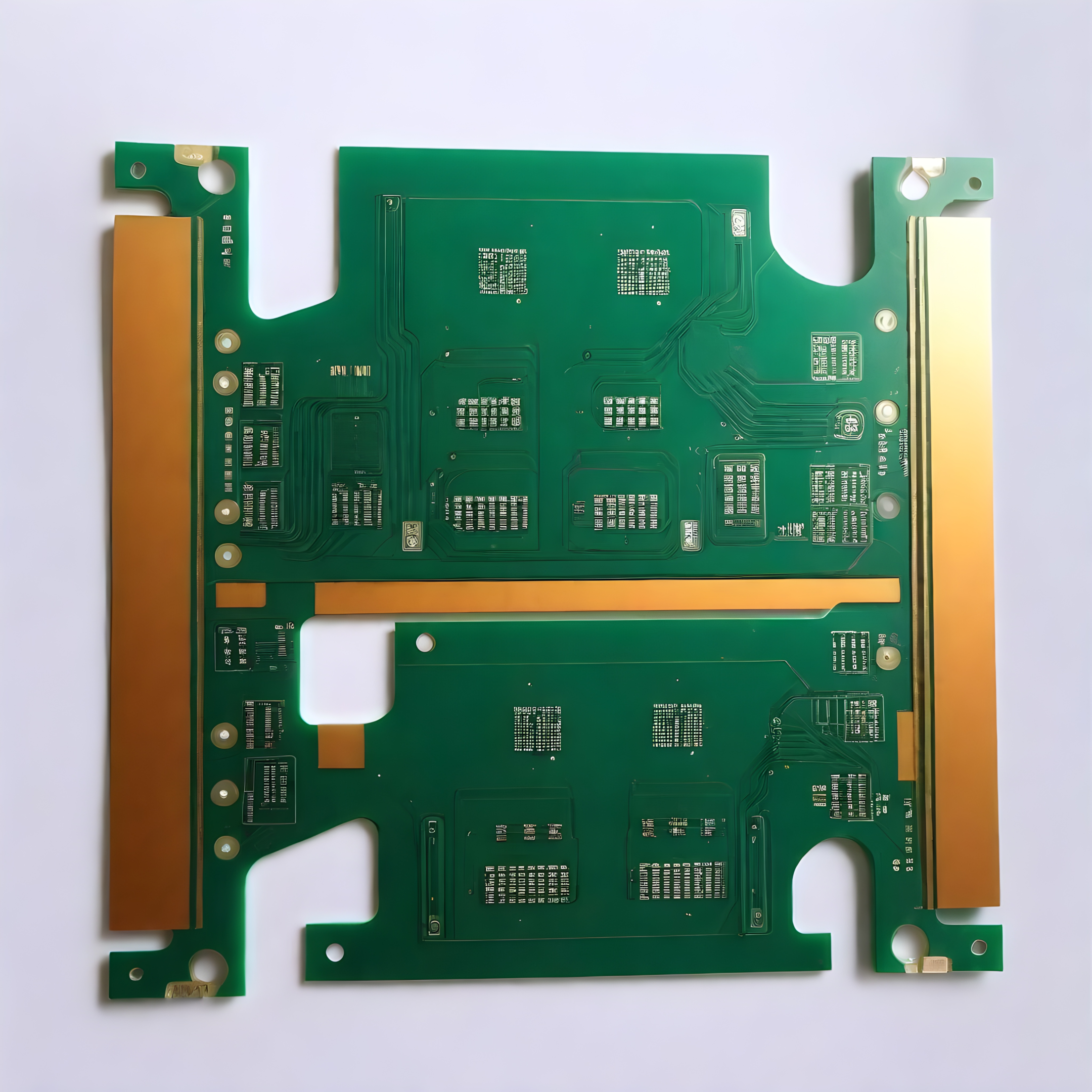
A PCB combining the features of both rigid and flexible pcb is used in advanced electronics that require rugged and flexible design solutions. Recent innovations have included better integration systems and well-heated thermal systems, which has led to efficient devices.
High-Frequency PCBs
Purposefully created for situations where there is a need for extremely high signal frequencies, which are made from materials like PTFE, which greatly reduces signal loss at high frequencies. they are very frequently employed on thorough communications strategy.
Aluminum-backed PCBs
Suitable for applications that require high power, this type of board has an aluminum heat sink as the back, which aids in thermal management. Recent works on this involve limiting heat loss from the surface as well as the design of lighter materials with the same or better performance.
HDI (High Density Interconnect) PCBs
HDI boards possess more separated spaces and lines, smaller holes, and stronger attachment pad density than traditional PCBS. The mainstream HDI technology provides the ability to achieve more functionality within a smaller space, offering the advantage of better electric conductivity due to enhanced via-fill materials with improved reliability.
3D-printed PCBs
Application of 3D printing in production of empty PCB minimizes processes that are resource-intensive and time-consuming but maximizes benefits like complex multi-layer design, cost reduction, and design flexibility. Besides, the eco-friendliness of this system can be mentioned; it is Ecological product manufacturing, as it consists of minimizing waste during the production process.
Ceramic PCBs
Advanced PCB boards with Ceramic Substrates (Aln pcbs and Alumina pcbs) are now becoming a preferred standard due to their excellent heat conduction and electrical insulation properties. These materials are compatible with high- power, ensuring that they perform and endure in high-thermal settings.
Material Considerations
The choice of material for blank PCB boards can significantly affect their performance.
- FR-4: is the most popular material, mainly because it is known for good isolation and high thermal resistance.
- Metal Core pcbs: Metallic core is utilized in LED lighting and auto quarters to regulate thermal performance.
- Flexible PCBs: Acrylic-based boards or polyimides are bendable and they used in places where there must be flexibility.
Applications of Blank PCB Boards
PCB blank boards are the most critical building blocks that automate the work of both prototyping and full-scale production. Here are the applications of blank PCB boards, summarized succinctly for each industry:
- Consumer Electronics: Used in smartphones, home appliances, and entertainment systems for the consumer.
- Computer Equipment: They are used in laptops, printers and other office products.
- Telecommunications: Important for routers, bridges, and communication network systems.
- Automotive: Designed as a component of engine controls, infotainment, and safety systems.
- Medical Devices: They are useful in pacemakers, imaging equipment and many other health technologies.
- Industrial: Provide operators with a detailed view of production and control it by taking on responsibility for machinery and industrial workflows.
- Aerospace and Defense: Involved in satellite equipment and in-cockpit-instruments in addition to defense systems.
- LED Lighting: Rated for LED applications by humidifying heat dissipation.
- Internet of Things (IoT): Enables to be in the IoT devices through that which they are connected and functioning.
- Wearable Technology: Pivotal for fitness trackers, smartwatches and other wearable devices.
Designing with Blank PCB Boards
PCB design process begins with the schematic capture and then the PCB layout, which entails the placement of the components on a blank PCB board, almost the way the circuit being designed appears. Here are some tips to optimize your design:
- Understand Board Limitations: Assess the shortcomings of the printable circuit board base material and the printing technology available to you.
- Component Placement: Arrange components to obtain efficient trace lengths and avoid potential interaction.
- Thermal Management: Make sure to design a heat dissipation system that operates well if it uses high-power components.
What is a blank pcb boards composed of?
Blank PCB (Printed Circuit Board) boards are primarily composed of the following materials:
- Substrate: The core structural layer, usually made of materials like FR4 (fiberglass-reinforced epoxy laminate), which provides rigidity and thermal stability.
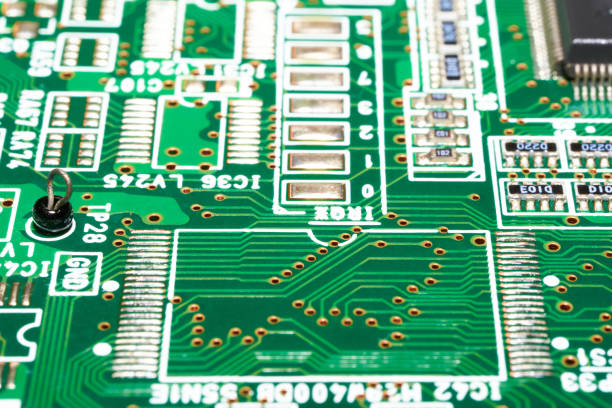
- Copper Layer: Thin sheets of copper foil are laminated onto the substrate. These layers are etched away to form the circuit patterns. PCBs can be single-sided (one copper layer), double-sided (two copper layers), or multilayered.
- Soldermask: A layer of protective insulating material, typically green, applied over the copper layer. This helps prevent accidental contact with the copper and provides resistance against short circuits.
- Silkscreen: White lettering applied on top of the soldermask for labeling component positions, which facilitates easier assembly and testing.
The significance of a Blank pcb circuit board
Blank PCB circuit boards form the structural bases in electronic engineering, where different components are designed and mounted for precise and steady connection. These are simple since one or more components that can be adjusted to fit certain requirements become smaller, cheaperand also expandable empty circuit board. By using blank PCBs, we can economize on organic compounds and protect our environment. Also, blanks enhance the reliability of devices and permit better heat distribution, a feature necessary for the proper functioning and prolonged life of electronic gadgets.
How do blank printed circuit boards work?
A PCB without any printed components (PCB) does not perform functions on its own but works only as the foundation of building working electronics. It is a mix of both the insulating materials and the conductive copper paths which form the printed circuit. Using this board, the electronic components can then be solder connections and these PCB designers can implement the routings of the signals and power of the device by following with a specific circuit design; therefore, the device can work properly.
Blank pcb Material Instructions
When handling blank PCB materials, follow these concise instructions:
- Storage: Store blank PCBs in a clean, dry environment to prevent contamination and moisture absorption.
- Handling: Use gloves to handle PCBs to avoid oils and dirt from fingers contaminating the surface. Handle by the edges to prevent damage.
- Cleaning: Before processing, clean the surface of the PCB with isopropyl alcohol to remove any residues or contaminants.
- Inspection: Inspect the PCB for any physical defects, such as scratches or blemishes, that could affect its functionality.
- Preparation: Prepare the surface for etching or applying photoresist by ensuring it is completely dry and free of debris.
- Etching: Follow specific etching instructions based on the chosen method (chemical etching or laser etching) to create the desired circuit pattern.
- Drilling: Drill holes for mounting components as per the design specifications, using a high-speed drill to ensure clean and precise holes.
- Final Inspection: After all processing, perform a final inspection to check for any errors or missed steps in the PCB fabrication process.
These steps ensure the PCB is prepared correctly for further processing and assembly.
Testing Of Blank PCB Boards
Testing the circuit boards with precise methods or verification before bringing them to the device assembly process is required. Here’s a flowchart that outlines the testing process for blank PCBs:
- Visual Inspection:
- First, make a thorough visual inspection of the machine to pinpoint the presence of any noticeable defects like scratches, missing or drilling parts, or misalignment.
- Dimensional Verification:
- Validate the dimensions of the PCB for compatibility with the specification. It includes the tabulation of the board thickness, fastener diameter, and board size.
- Copper Thickness Measurement:
- Define that the copper foil thickness on the PCB is within the acceptable tolerance range as recorded for the specific project.
- Solder Mask Adhesion Test:
- The adhesion test of the solder mask and solder material by the tape adhesion test is needed to check if the melting solder mask is firmly positioned onto the aln PCB surface parts.
- Electrical Testing:
- Carry out electrical tests so that the connection and insulation of the system are distributed. Primarily, this can be done through either a flying probe tester or by using a bed of nails tester.
- Microsectioning (if necessary):
- At some stage, the cross-sectional analysis could be conducted to verify the depth of the internal layers, vias, as well as the position of the position of the components to make sure that they are not disconnected or misaligned.
- Thermal Stress Test:
- Thermally cycle the PCB in the product to make certain that it will be able to respond to the temperature changes that it will face while in operation.
- Final Inspection:
- Carry out the total outstanding study at the end just to show that all the previously obtained points are validated as pre-approval for the PCB assembly.
- Report Generation:
- The performance test should be duly documented, and a report should be made. A conclusion should make a point of including the test results, what standards were not met, and providing a summary of all tests conducted.
Benefits of Blank Circuit Board Testing
Testing blank circuit boards provides several critical benefits:
- Quality Assurance: Ensures that each PCB meets the required quality standards and specifications before components are added.
- Error Detection: Identifies manufacturing defects such as shorts, opens, and improper etching, which can be corrected before further processing.
- Cost Efficiency: Detecting defects early in the manufacturing process reduces the cost of rework and prevents costly failures in final products.
- Reliability Improvement: Testing contributes to the overall reliability of the finished product by ensuring that the foundation (the PCB) is defect-free.
- Process Validation: Helps in validating manufacturing processes and materials, ensuring consistency in production.
- Compliance: The PCBs are tested and standardized to match industry specifications and company requirements. This mitigates the level of compliance issues and penalty charges.
- Customer Satisfaction: Customer satisfaction goes up since the products function correctly as specified and do not fail anywhere; that is, their brand reputation is sound.
Blank pcb board Testing Methods
Therefore, testing of blank PCB boards involves several methods to rule out defects that could hamper their function if they do not meet the desired quality and functionality standards before further processing and component assembly. Here are concise descriptions of common testing methods:
- Visual Inspection: Check the board for physical defects like scratches, cracks, and incomplete punching. Sometimes this is the very beginning of quality control work.
- Microsectioning Analysis: By using this method, one can do a visual examination of internal features like layer integrity or via’s quality using a microscope.
- Electrical Testing: The present checkup can be done with the help of a bed of nails tester or a flying probe tester if possible to detect existing problems with regard to the proper electrical connection as well as short circuits or open circuits on the PCB.
- Time Domain Reflectometry (TDR): The TDR technique can be used to measure the reflection of signals on the PCB traces, whose analysis aids in locating and identifying the causes of discontinuities in impedance variations.
- Automated Optical Inspection (AOI): Spending an AOI machine to see defects on the surface of PCB, such as paths thinning or excess copper thickness, is a superior productivity enhancement.
- X-ray Inspection: Introduce X-ray technology at the surface to review internal detailing and layer alignment; this is particularly applicable with multilayer PCBs and the matter of hidden defects like internal delaminations or mismanaged via fills.
- Peel Test: Perform a peel test for the copper layers to ensure they are sticking strong to the substrate and that the adhesion is according to what the thieves established.
- Solderability Test: Conduct a solderability test that determines the capability of solder to attach nicely to the PCB’s surfaces, which is of primal importance in the processes to follow.
Challenges & Limitations Of Blank PCBs
Here’s a concise summary of the challenges and limitations associated with blank PCBs:
- Complexity in Design: Another flex PCB that has a multi-layer configuration gets some accuracy issues for a design fabrication as well; it has been found to be unstable in terms of the integrity of the signal propagation.
- Thermal Management: Heat management problems in powerful electronic circuits or high-frequency signal spot changes are a critical issue, and often you need to use metal-core PCB material, which is more expensive as a rule.
- Material Limitations: As an array design, FR-4 and these particular materials offer the possibility of functioning in those frequency and temperature ranges, which will not be extreme, and those advanced arrays, which are costly, can also be used.
- Manufacturing Defects: Peculiars like short circuits, open circuits, or misalignments would be very tiring, so they will have to be cured. There is a greater chance you will have to ensure quality inspections.
- Durability Concerns: Through loads such as H20 and high temperature changes, TRS components may get destroyed when left in this state for a long time.
- Cost Considerations: The less PCBs need the advanced and costly material and method of practice focused on in a purely professional manner only.
- Regulatory Compliance: Following regulations relating to the environment makes the design process even more sophisticated and may, sometimes, cause certain limitations in the materials used, which then affect the design and cost.
They, due to their narrowness, provoke complicated constructions and exact methods and materials. To succeed in it, these will plausibly have to be pretty innovative, and what else is needed is growing demand.
Conclusion
Bare PCB, which are the boards to be printed on, are not merely the components that are out of sight and in the background; rather, they are the stage for the production of state-of-the-art devices and imaginative creations in the domain of devices or electronics. Whether material is being overcomplicated or oversimplified, it’s crucial to notice places where it is being used in this way. For whatever your position might be—being an engineer, a student, or a DIY person—eventually you will be defeated by the blank PCB board challenges, but instead of that, your list of electronics design—a total design declaration—achievements will be longer than ever.
Citing the PCB boards leads the readers to some obvious advantages of electronic devices. So, the foundation stone is found and developed into higher inventions, and you do it yourself on a on a multilayer PCB.