The printed circuit boards (PCBs) are the foundation of almost every electronic device, and of course, they are the main pieces tying up all components so well that they truly perform a function and do it reliably. Among all other elements that contribute to PCBs, the pads stand out as being one of the most vital, yet they seldom get the recognition they deserve.
In this article, we will take a look at what PCB pads are, the different types of PCB pads available, and the importance of PCB pads in the design of circuit boards.
What are PCB pads?
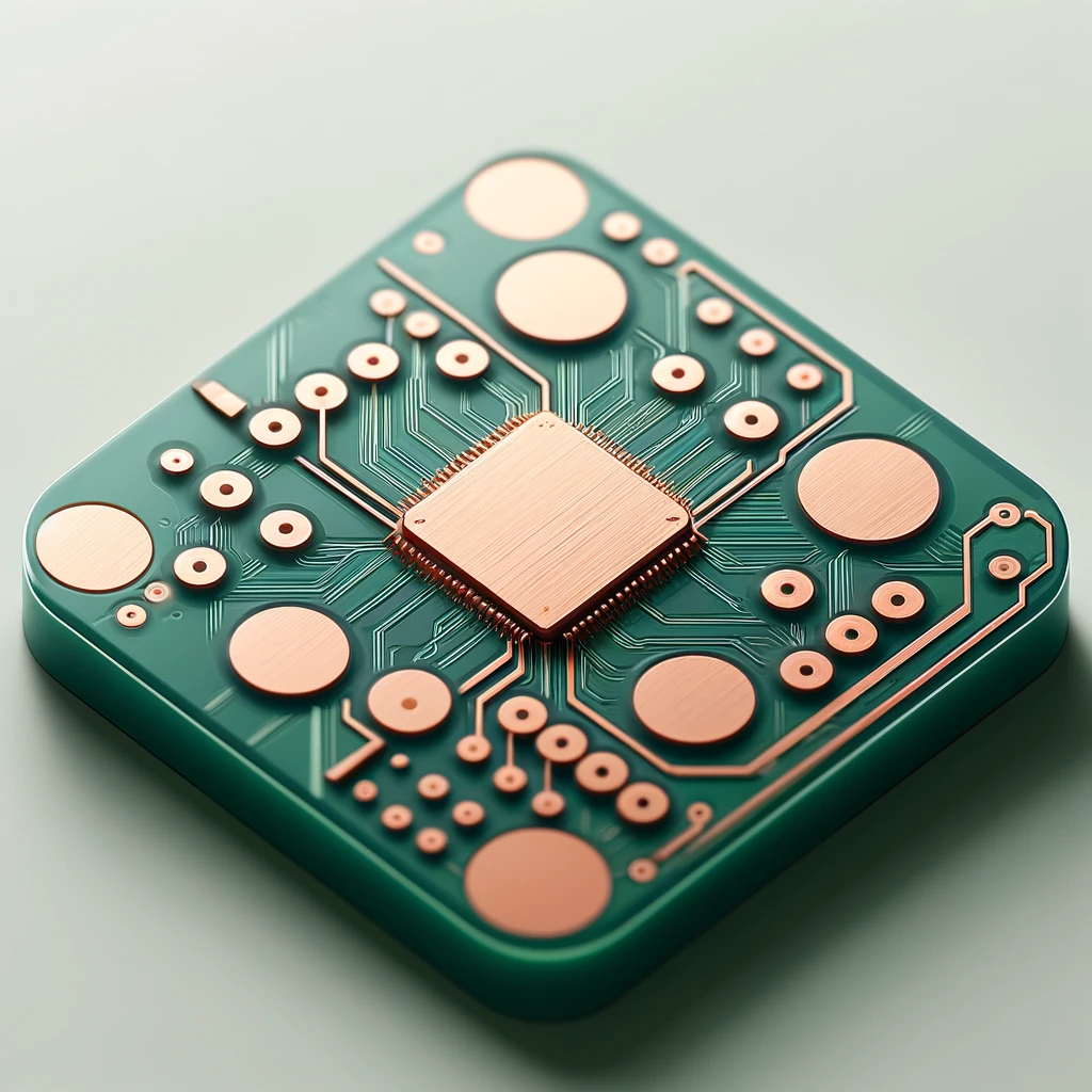
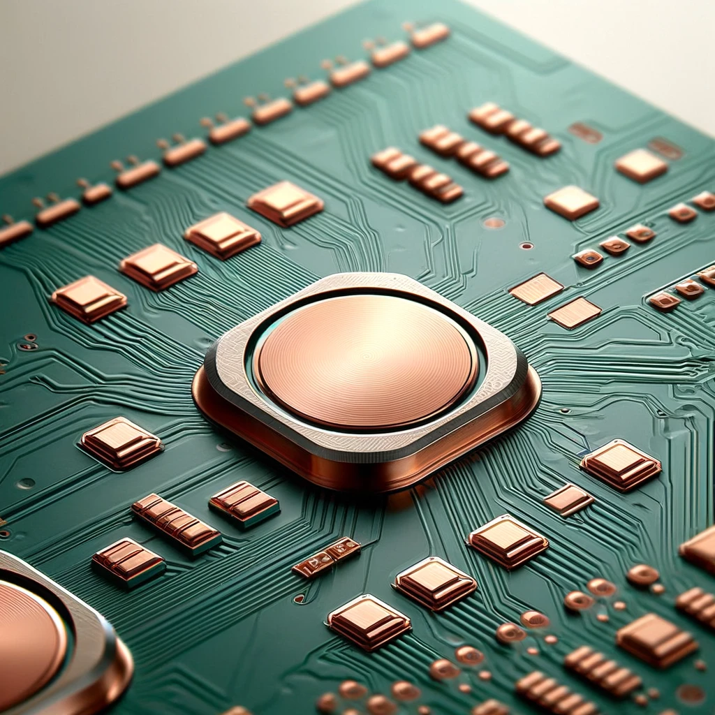
Pads of printed circuit board placed on a PCB are the small, metallic setups where components are soldered. It is these pads that carry both the leads of components like resistors, capacitors, and IC’s enrouted to their respective spots on the board just like the solder mask defined pads. The main role of a pad is to offer not only mechanical but also electrical connections for the mentioned components as well as for the devices to be installed on top.
Types of PCB Pads
There are several types of pads used in PCB design, each tailored for different applications:
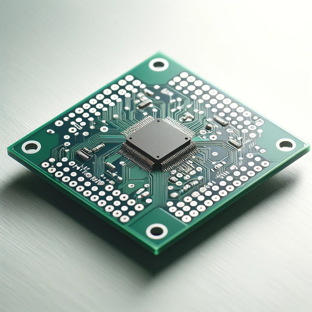
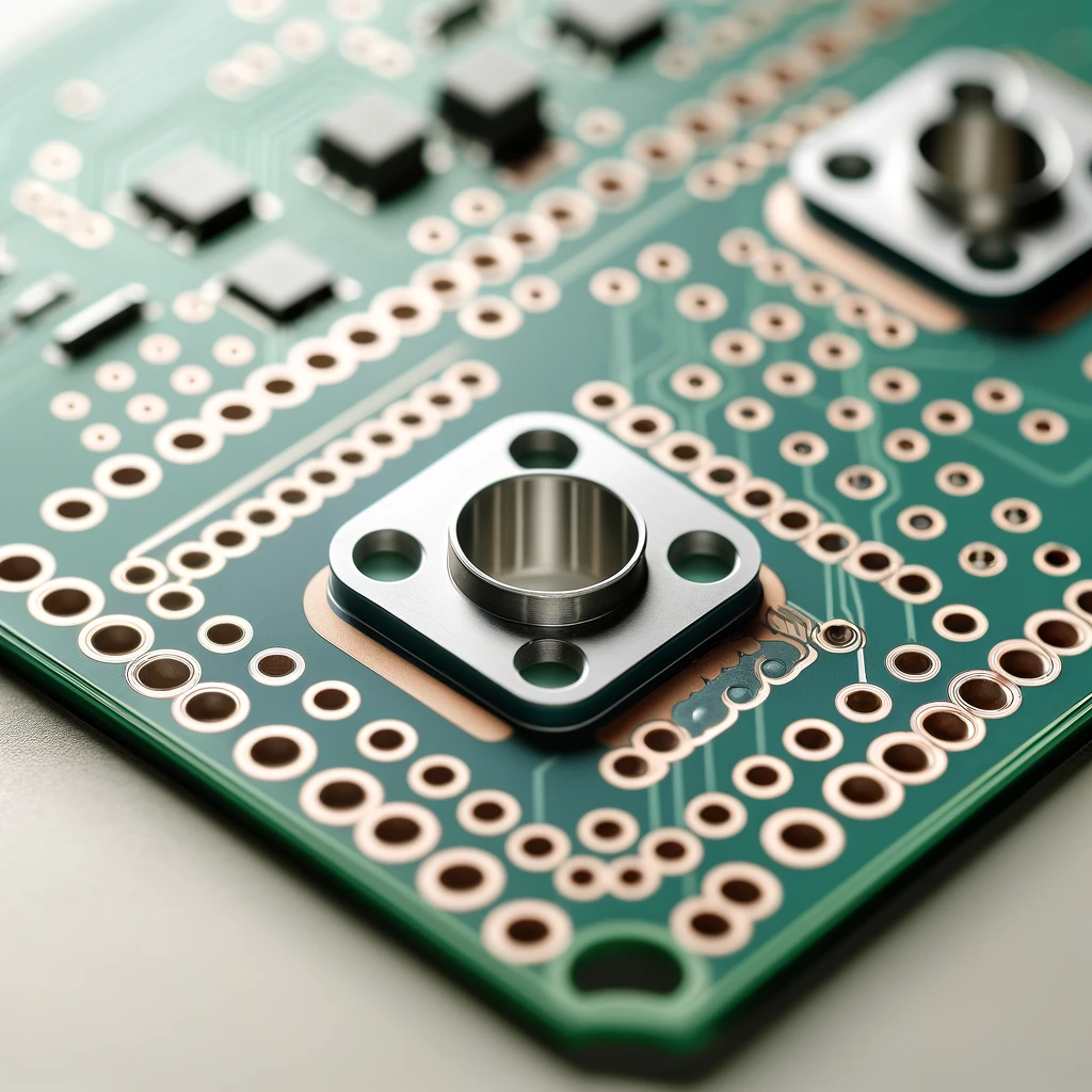
Through-hole Pads
They play a critical role in standard through-hole circuit technology, wherein component leads are inserted through the pre-drilled hole on one side of the PCB and then soldered to the pads created on the reverse side of the PCB to mount through hole components. Copper tracks are reliable with a solid mechanical coupling, which makes them perfect for circuits involving physical stress.
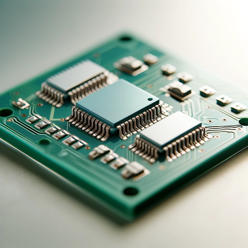
Surface-mount Pads
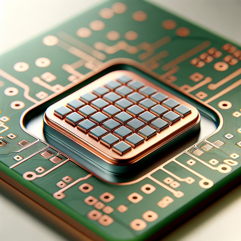
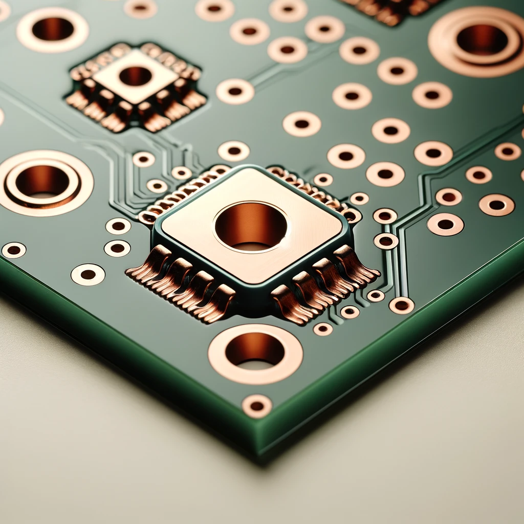
Surface-mounted technology (SMT) is a process involved in components that are directly mounted onto the surface of the printed circuit boards in surface mount components. The smd pads is not spread complexly, but they are flat and have a flat rectangular shape so as to help parts maintain their place with a little amount of solder called surface mount pads.
Connective Pads
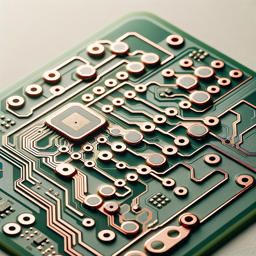
These pads function as connection point screw terminals to the different layers of a multilayer PCB. Those are via in pad, which is a name for vias that do the job of connecting a signal from one layer to another.
Test Pads
These are used only for the purpose of tests that are related to the watertightness and accuracy of the whole PCB during and immediately after manufacturing. Test pads are the places where the component is not attached directly; instead, they are essential for creating a complete connection between the component and circuit.
The Size and Spacing of the PCB Pad
Where the size and spacing of the pads on the circuit board design are important, they are the determining parameter that can be used to measure success levels of both assembly process and performance of the circuit board.
Size
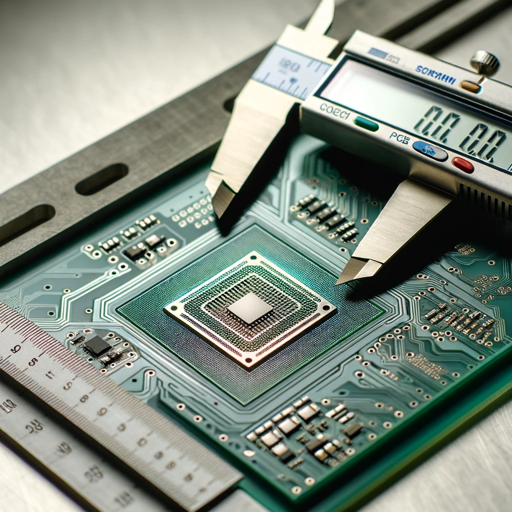
The pad size should be sufficient to allow good solder coverage and mechanical support; however, a size too large should be avoided to prevent solder bridging or interfering with adjacent pads. The lead-size terminals are countered by the pad size evenly.
Spacing
Spatial gaps between the stacks must take care of electrical shorts and not allow insufficient isolation of conductors. This pitch, which is subjected to the level of voltage and density of the circuit, determines the lead through the circuit, which is the impact of space when a transaction is conducted. Signal integrity will be better, and there will be no chance of solder bridging that happens when components are put on the boards due to good spacing designs.
To achieve PCB reliability and manufacturability, blind/buried vias bga pads with geometric characteristics such as size and pitch must follow accepted design rules and recommendations.
Significance of Pads in PCBs
Pads on PCBs are crucial for several reasons:
- Connection Points: The pads are the most important interface components for the soldering of components on the board, securely and firmly bonding those components with the board as required.
- Signal Integrity: Stabilization of the signal is achieved by using the correct placement and design of pads; interference is effectively eliminated since noise can no longer affect the signal.
- Heat Dissipation: The pads facilitate effective heat dissipation and consequently thermal management of the board by dispersing heat from the added components thermal and mechanical stresses.
- Testing and Debugging: The special test pads are made in such a way that it’s easy for the operator to press the buttons and tester during the work and after the assembly to figure out the component fault.
Role of Pads in Circuit Design
Implementation of a PCB gap is of critical importance in the whole process of building the circuit board. Here are some key aspects influenced by pad design:
- Electrical Connectivity: Pads should not only be constructed to support proper electrical contact between a board and its components but also to prevent any damage or deflection throughout their service life. The integrity of the power links greatly depends on the pad quality. Even an imperfect pad may cause the device to become defunct if it loses contact.
- Heat Management: The heat, in turn, arises from the electronic components circuits that come from operation. Conductive thermal grease and metal pads facilitate an efficient thermal path, which is good for keeping circuitry components colder.
- Signal Integrity: The amount, shape, and design of the circuit pad lie at the heart of the validity of the electric signals that go through the circuit. Such specifically created pads suppress noise and interference to ensure the transmission of voice over clarity.
- Durability: For instance, as is common in through-hole structures, pads make up a large portion of the mechanical strength of the joint. A good pad design should have features that will keep it physically unbroken without the electric contact getting affected.
Problems Caused by Wrong PCB Pad Sizes
Properly sized PCB pads may cause the board to suffer some problems, which means it won’t work well and you can’t be confident in its sustainability. Smaller pads will possibly not allow the solder to build proper joints with sufficient kilograms, as the result would be weak joints, which are vulnerable to fracture. The failure of circuits with irregular intervals or permanent reasons can also appear. The problem, however, is that if solder excess is too much, like too many pads, it will accumulate between the pads and cause short circuits, which leads to solder bridging and conductive pathways between pads and conductors. A variation in terminal or assembly position is not always guaranteed to maintain signal integrity, causes components to have lower performance, and creates the possibility of misfunctioning, which calls for replacement and negatively affects the overall quality of the product.
There are two types of PCB pads
PCB pads can primarily be categorized into two types:
Through-hole Pads
These pads are used in the through-hole technique, which features leads that pass through drilled holes in the PCB and are soldered to pads on the opposite side of the board. They offer good mechanical locking and are thus best for those components that are analogous to the physical bond.
Surface-mount Pads
A kind of SMT is used for such pads where components are mounted right on the top of the PCB. Flat and miniaturized surface-mount pads are an inherent element of today’s compact electronic assemblies. They are commonly referred to as through-hole pads. The use of SMD (surface-mounted devices) technologies enables higher component density by maximising the surface area of the board, but the mechanical strength of SMD is lower than their through-hole counterparts.
Design Considerations
When designing PCB pads, several factors need to be considered to optimize performance:
- Pad Size and Shape: There must be connectors of the appropriate size and shape for a good alignment with the lead-in component. Excessively large kits or too small kits could lead to wobbly joints or the inability to solder.
- Material: Copper takes over pad functions because of its perfect electrical conductivity and heat power copper pad underneath.
- Placement: Pads have to be precisely positioned close to the componentary leads and other circuitry to ensure that they are correctly aligned. The misalignment can cause short circuits or open circuits in the work.
Conclusion
In general, PCB pads are not only the places where the components are attached; they are also very important in enabling the functionality and dependability of every electronic gadget. Knowing their role will, therefore, enable better management of PCBs, which will result in the PCB designs being more effective and robust fine pitch bga chips. Whether you are a professional engineer or an enthusiast, understanding the nuances of PCB pad design can elevate your skills to an expert level in circuit design, which will, eventually, allow the development of quality electronic products.