Discover the fascinating stack-up design for printed circuit boards in PCB stack-up design guide. Explore stacking up in an airboat multi-layer circuit board, look at all the signals and possible factors to consider for the design, and find tips for better performance and reliability. Whether you’re an expert engineer or a novice, our guide is designed to give you a comprehensive understanding of all the considerations involved in PCB stack-up design.
What is a PCB stack-up?
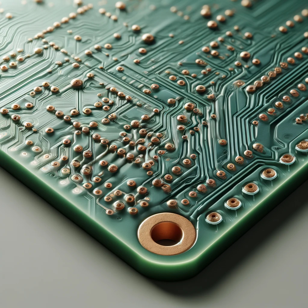
PCB stack-up is synonymous with the position (location) and organization of all the layers that make up the top layer of a printed circuit board (PCB). PCBs comprise multilayers of various materials laminated to form a uniform structure as one PCB board. Configuration of surface layer of the top layer pcb stackup determines the sequence, constitution, and features of these layers that are of critical importance for the electrical features, signal integrity, and mechanical strength of the PCB.
The Role of PCB Stack Up in Circuit Board Design
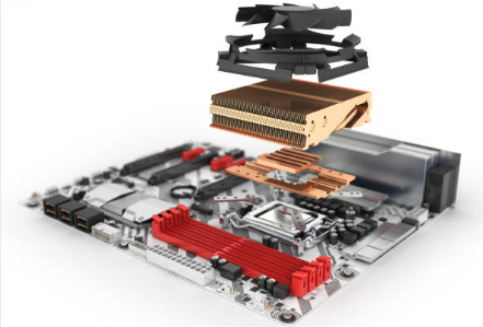
PCB stack-up is the basis of circuit board design, with it being a key component that not only determines the operation of the device but also its performance and reliability. Through the process of stacking conductive traces, insulation materials, and ground/power roots, the layer by layer layout assembles factors that contribute to signal integrity, power distribution, and thermal management.
Different Types of PCB Stackup
In PCB stacking, substances such as copper layers and insulating layers are organized to form a PCB. Here are some different types of PCB stack-ups:
Single-Sided Stack Up
This is the most simple PCB, made of only one layer of substrate and one layer of conductor. All electric parts and elements are put together on one side of the board.
Double-Sided Stack Up
This kind of PCB has conductive material on both sides of the board. Placement of components on both sides of the board is achievable, which opens doors for more complicated circuits.
Four-Layer Stack Up
A four-layer PCB layout is made up of four layers of conductive material. In most cases, these are two signal layers and two power or ground layers of the PCB. Extra layers allow for better trace routing and lessen EMI noise as well.
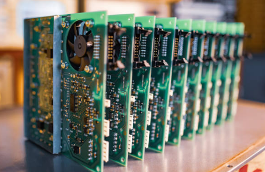
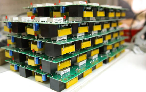
Multi-Layer Stack Up
The number of conductive layers on multi-layer PCBs normally varies between 4 and 16 and more. These are, for example, used on the motherboards of electronic circuits such as computers or satellites. More tiers ensure plenty of room to incorporate signal routing, powering, and EMI in the design.
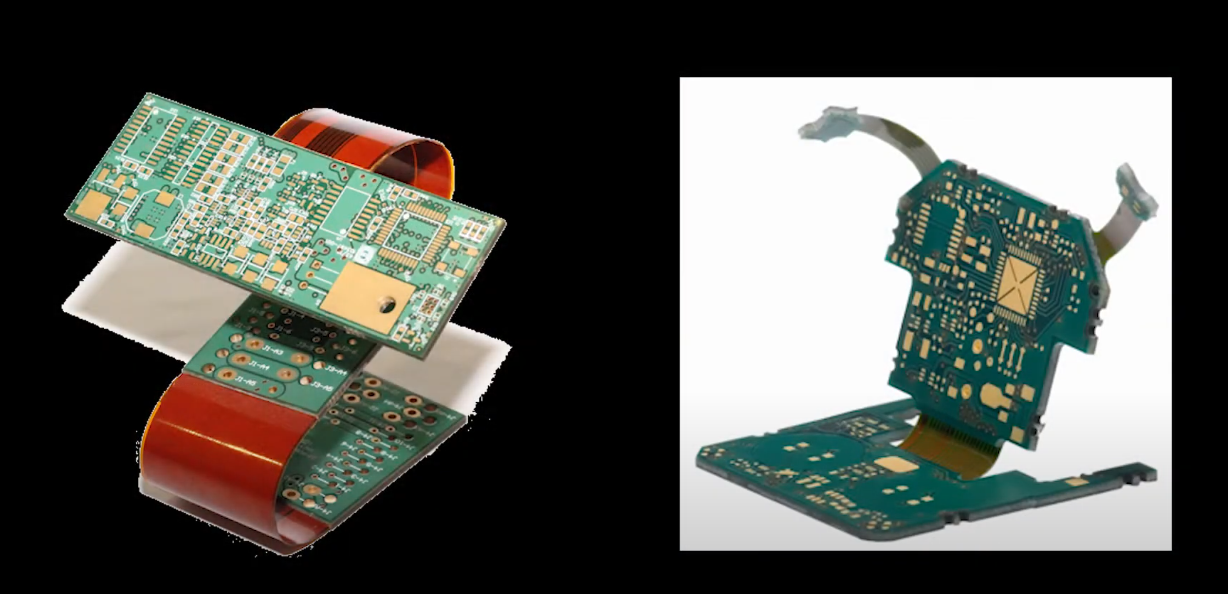
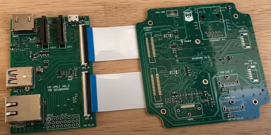
Rigid-Flex Stack Up
This PCB concept uses both rigid and flexible PCB technology. It consists of many soft, flexible layers of circuit substrates attached to the hard exterior layer. Rigid-flex PCBs are applied to various systems where flexibility plays a key role.
High-Speed Stack Up
PCBs of high-speed type are fabricated to bear high-speed digital, RF, or microwave quantities. These stacked PCBs are considered spent once they have been thoroughly analyzed to determine their impedance, amount of signal loss, and EMI level.
HDI (High Density Interconnect) Stack Up
HDI PCBs are analytically characterized by a high density of components and interconnections. The stack-up consists of blind and buried vias, as well as micro vias, and is commonly used in portable devices such as iPhones and tablets.
UNDERSTANDING THE LAYERS IN A PCB STACKUP
The PCB is generally composed of multiple layers of different materials which are laminated together. These different layers are assigned different roles that are significant for the background and quality of the PCB. Here’s a basic overview of the typical layers you might find in a PCB stack-up:
Top Layer (Signal Layer)
- This layer consists of the signal traces that are interconnected between different elements of the PCB. Most parts are usually soldered over the pads on the board.
Inner Signal Layers
- PCBs can have multiple layers stacked sandwiched between the upper and lower layers, which are frequently used for making additional signal traces. The number of inner plates we use depends on how complicated our design is.
Power and Ground Planes
- The power and ground planes are layers that that serve as power and ground connection points for the components on the circuit boards. These power planes are responsible for balancing the distribution of power and lowering electromagnetic interference (EMI) and noise from the circuit.
Prepreg Layers
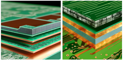
- Prepregs are insulating layers made from glass fiber-woven cloth which are soaked in epoxy resin. They play a role as an intermediate and insulating element between the copper layers.
Core Layer
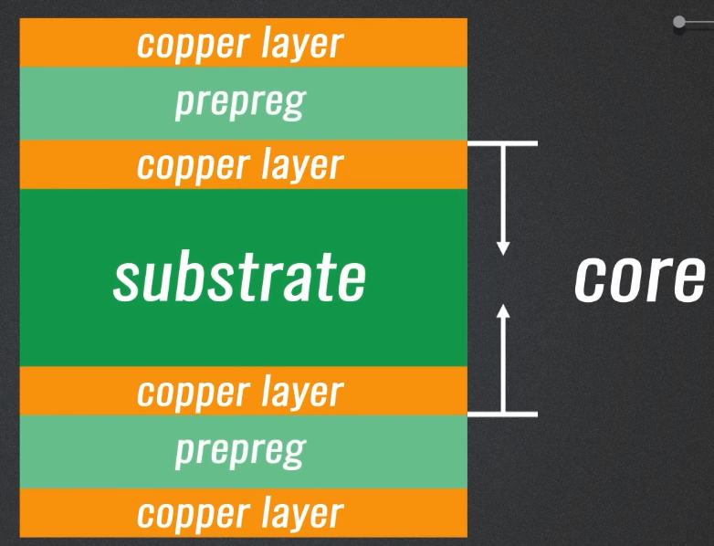
- The core, which is located at the center of the PCB stack-up, is usually a fiberglass-reinforced epoxy laminate. It provides the necessary mechanical strength to the PCB and serves as a fundamental layer for the inner copper elements.
Bottom Layer (Signal Layer)
- In the same way as with top layer, the bottom layer is made up of signal paths and their pads. It forms the soldering layer of the circuit board.
Solder Mask
- The solder mask is a layer that is placed over the both bottom and top copper layers. This protects the traces and stops any soldered bridges forming during assembly. Generally, it is green, but it also uses various colors for identification or embellishments.
Silkscreen
- The silkscreen layer contains marks, labels and, at the same time, component outlines that are printed on the PCB board for further assembly and identification. Generally, it’s one of the color white.
DESIGNING EFFICIENT LAYER ARRANGEMENT IN PCB STACKUP
Efficient layering in a PCB (Printed Circuit Board) stack-up is vital because it dictates the quality of digital signals used within the internal parts of your design. Here are some key considerations and steps to follow:
Understand Signal Types and Requirements
In stack-up design, different signals, such as digital or analog as well high frequency signals such as the high speed signals will have varied peculiarities and hindering drawnbacks that need to be set into consideration.
Consider Ground and Power Planes Distribution
The stack-up layout should comprise dedicated power and ground planes or polygons to allow low-impedance paths for the power and return currents, respectively.
Manage Electromagnetic Interference (EMI)
EMI management is revolutionized by the PCB stack-up design, which gives a shielding operation and lowers electromagnetic radiation.
Plan your design requirements to ensure manufacturability
Clearly outline electrical and mechanical requirements. This entails the kind of board, the nature of the material, the design aspect that provides multiple layers of signal and power, as well as the power delivery network (PDN) and its impeadances characteristics, impedance specified for high-speed tracks, the position of the routes that are supposed to maintain a controlled impedance, the analog and digital circuitry which are supposed to operate at a high frequency, the routing signals other connections whose position is
Understand the manufacturing tolerances before finalizing the layer stack
Under intense strain and heat that occur during manufacturing, the material undergoes significant amounts of mechanical and thermal stress. With this non-aligned outer layer, of the outer layer count the case and an offset of the vias may become possible.
Essentially, the type of materials chosen and their proper arrangement between the levels is the driving force behind the built up efficacy rf components. Ensure the talks happen in early stages with the manufacturer to know what their capabilities and limitations are. This holds back the time it takes to create the prototype, and it also allows a smooth switching stage from the prototype to mass PCB production.
Stack-ups with Both Power Plane and Ground Plane
Multilayer PCB stacks with power as well as ground planes are especially crucial for power distribution and signal transmission with reference to the electromagnetic problems encountered in electronic devices. Surface-mount devices (PSDs) or Power planes connect component power supply pins and rigid substrate has appeared, carrying DC power from power source and creating stable operating environment. However, the solid ground plane or planes are are formed by the backside side of surface mount devices that serves as signal reference planes and minimizing noise and simply providing a low-impedance path for returning currents. The constellation of power-ground plane pairs is responsible for holding such a conveyance of controlled impedance along the signal routes, which, in turn, causes a great reduction in reflections and control impedance and mismatch. These planes are capable of achieving these objectives through filtering high-frequency noise as well as voltage surges and consequently smoothing clean power delivery through decoupling capacitors. Furthermore, power-ground plane pairs constitute shields as well, when such functions shield internal electromagnetic fields and, as a result, minimize electromagnetic interference emission and susceptibility. In this situation, thoughtful attention to the arrangement of the power and ground planes is of fundamental importance. The aim is to obtain the best performance results, perfect reliability and electromagnetic compatibility.
THE ROLE OF PREPRAG IN PCB STACKUP
Prepreg, abbreviated as “pre-impregnated,” is one of the most vital parts of the PCB stack-up process. It serves several essential functions: It serves several essential functions:
- Insulation between Copper Layers: Prepreg is density composite constructed of glass cloth fiber treated and saturated with epoxy adhesive. It is located among copper layers of the PCB stack in a gap between layers to separate one layer from another based on capacity requirements. This isolation prevents that all electrons, instead of only travels where it are intended, from taking shortcut.
- Adhesion and Lamination: Preg layers work as the primary adhesive material, comprising all materials during the lamination stages of the PCB process. During the conduct and curing procedure, the epoxy in the formation of conductive fabric is softened, causing the copper layers and core to become a strong and dependable permanent circuit.
- Thickness Control: Prepreg’s sheets are manifold in thickness; thus, the RT designers have the possibility to define the thickness of the board’s stack-up. Using prepreg materials of different thickness ranges, camera designers are able to precisely control dielectric spacing between copper layers and moreover its proper impedance, signal integrity, and circuit manufacturing, which, in terms of its consistency, is very important.
- Mechanical Support: The prepreg layers of the circuit board serve as mechanical reinforcement in the constructional structure of the board. Synthetic fiber and fabric provide the PCB with robustness, making it resistant to bending, warping, and mechanical stress caused during handling, assembly, and when in use.
- Thermal Properties: Thermal properties of prepreg materials may contribute to the overall better thermal performance of the PCB. They take away heat from the components or their operating space, thereby preventing them from ever getting hot or unstable. Choosing the prepreg material with adequate thermal conductivity and heat-dissipation property is the paramount part of ensuring the successful thermal management of the electron apparatus with a high capacity.
Prepreg turns out to be a decisive feature of PCB fabrics and their performance. It is the insulation, adhesion, thickness control, mechanical support, and thermal management which help to achieve reliable and functional PCB which can further be manufactured to current industrial standards. Specialists, however, should meticulously consider the material inputs into the stack-up design so that each PCB project is achievable.
CONSIDERATIONS FOR HIGH-SPEED BOARD DESIGN IN PCB STACKUP
For high-speed applications, when the PCB stack-up design for board density and thickness is under consideration, several critical factors must be taken into account. Otherwise, signal integrity, electromagnetic compatibility (EMC), and the general performance of the PCB layer stackup will not be satisfactory. Here are some key considerations for high-speed board design in PCB stack-up:
- Layer Arrangement: Designs with high speeds may need multiple signal tracks that are properly impedance controlled. Signal layers are alternately set between anything that is power and ground planes to create something that cancels out signal distortion and lessens EMI at the same time.
- Impedance Control: Control of impedance within the speed signals at the interface is a vital necessity to avoid reflections and maintain the integrity of the signals. Materials shall be carefully chosen, keeping some factors in mind, such as specific dielectric constants and thickness, to make sure the proper impedance levels are achieved for signal traces.
- Signal Integrity: The proper wiring techniques, e.g., matching-length traces, differential signaling, and avoiding sharp bends or corners, are the keys to conserving signal integrity in fast signal designs. Also, the number of vias and the positioning of those vias are other factors that minimize signal connections and impedance distortion.
- Power Distribution and Decoupling: High-fidelity designs usually indicate good power sourcing and, therefore, stable, clean power delivery to sensitive components. The power planes of the desired design must support low-impedance reference planes all over the circuit, with decoupling capacitors in practical places of the PCB structure being used for this purpose to help filter out high-frequency noise and voltage fluctuations.
- Grounding: Grounding must be accurate in the implementation of a broad board design process to avoid difficult ground bounce, which may result in increase of noise in the circuit. Proper grounding techniques must include, for instance, the star grounding method and minimizing loops to have a stable reference plane for disturbance paths and EM frequency reduction.
- Stack-up Symmetry: Preserving the symmetricity of the PCB stack-up directly acts as a shield from the signal skew and impedance mismatches between the signal layers. When the routing layer width and thickness are identical in all metal pieces and the copper’s weight are balanced, transmission of the signal is enhanced and signal distortion is minimized.
- Dielectric Materials: The selection of high dielectrics which have low loss tangent and evenly electrical properties serves as a basic requirement for high-speed circuitry designs. These materials are mainly meant to reduce signal attenuation and let users work with signals of varying frequencies with similar signal behaviors at these frequencies.
- EMC Considerations: The fast-clocked designs are potentially affected by electromagnetic interference (EMI) and emissions. The shielding techniques proposed, like the implementation of solid ground planes and the addition of extra ground layers for dissection, act as viable measures to fight against the EM and thus the ECMs requirements.
The Importance of Quality Assurance in PCB Stack Up
Quality control for PCB stack-up is critical to this effort in terms of the durability, dependability, and efficiency of printed circuit boards. It ensures that the design of stack-up satisfies the specifications of controlled impedance, layers, and thickness and also holds the property of materials which are necessary to maintain signal integrity and resist signal distortions. QA completes not only the design validation but also the manufacturability verification by analyzing the drawings and schematics for any potential errors that could result in issues during fabrication. Through extensive checks and assurance, QA is able to achieve reliability, robustness, and compliance with electromagnetic compatibility (EMC) standards at the best costs average, meeting the expectation of its customers. In the end, QA is the key issue in the production of top-quality PCBs that meet requirements on the regulators’ side and the customers themselves.
Common PCB Stack ups for a Four-Layer Board
For a four-layer board, most of its stack-up configurations are the widely used ones, mostly developed to suit particular designcharacteristics and operational considerations. Here are two common stack-up configurations:
- Top Layer (Signal Layer):
- This layer is where we place most of the main traces, component pads, and routing for all the electronics to take place.
- The circuit is designed at this level, and the components are put and soldered on different pads. The signal traces are utilized to link the different parts of the circuit.
- Inner Layer 1 (Ground Plane):
- The first inner layer, the ground plane from a solid surface, also helps to perform a low-impedance path for returning currents and to avoid EMI (electromagnetic interference).
- This layer is helpful to reduce noise within the circuit because it is also good at guaranteeing signal integrity by adopting a reference plane, which covers signal traces on both sides of the PCB.
- Inner Layer 2 (Power Plane):
- The second inner layer often plays the role of the power plane, which makes the power distribution through the different sections of the circuit possible.
- This layer allows you to reduce power drops, ensure power transfer and perform good thermal management, that is often done by spreading heat from components.
- Bottom Layer (Signal Layer):
- As as the top layer, the bottom layer consists of signal traces, component pads, and routing for the circuit and component leads.
- These traces mark out a copper board and provide routes over the whole thickness of the board from Vias. This kind of internet interaction facilitates human relationship formation regardless of one’s physical presence.
Four layer stack-up ensures that in many PCB designs there is approximately effective performance, price and manufacturability of two layer board only. Such an arrangement provides sufficient routing flexibility for signals, besides decreasing the EMI and maintaining signals integrity and power distribution stability through the various ground pins and planes. Fundamentally, this 2-in-1 finger is quite production-friendly and offers excellent heat dissipation.
Instead of normal four-layer stack-up, there could also be the variation curve in which the two inner planes are being swapped between the ground and power planes or two signal layers along with multiple ground planes are utilized in the inner layers instead of the inner two ground planes alone. Obviously, the inner layers are generally decided according to a specific design demand, such as high-speed signaling, mixed-signal applications and power distribution.
The Impact of PCB Stack Up on Electromagnetic Compatibility (EMC)
The stackup of PCB affects EMC (Electromagnetic Compatibility), which is the definition of an ability to cooperate for other devices to operate without interfering with each other and not being affected by internal layers of external electromagnetic interference. Here’s how the PCB layer stack up make-up influences EMC:
- Grounding and Shielding: The use of proper grounding points and the inclusion of a ground plane in the provided PCB transfer scheme create an impedance path of low power for return currents, minimizing noise from common modes and ground loops formation. The PCB components and the circuits are responsible for creating electromagnetic signals, which, when confined at the surface of ground planes, help reduce electromagnetic interference (EMI) emissions and susceptibility.
- Signal Integrity and Crosstalk: The stack-up of signal layers, ground plane, and power planes in the PCB underlies directly the odds of signal integrity and crosstalk. Paths of signals routed between adjacent ground planes experience the best performance when they are backed by a solid reference plane; thus, we can expect minimum of signal distortion and lower risk of crosstalk. Controlled impedance and reduced signal reflection of the trace enable clean signal transmission, which help in minimizing electromagnetic emission and, in turn, decreasing susceptibility to external interference.
- Power Distribution and Decoupling: In the PCB stack-up, PDNs adopted through power planes carrying power supply stabilize and yield clean power at the components level. Decoupling capacitors are very special components that filtered away from the circuit at particular points. They help with clean power delivery and minimize electromagnetic lines from power traces.
- Layer Symmetry and Impedance Control: Symmetric PCB stack-ups can be obtained with balanced layer construction and controlled impedance. It eliminates signal skew and impedance mismatch possibilities, which can lead to signal distortion and larger external interference. Preservation of symmetry in the stack-up allows transmission and reception of signal waves with uniform angles of incidence; thus, in the end, EMC problems are reduced.
- Material Selection and Dielectric Properties: A selection of the materials and properties of dielectric in PCB assembly would be a key factor in enhancing the EMC performance. The presence of high-quality dielectric materials which have loss tangent and a low and consistent electrical property leads to the minimization of signal attenuation and the simultaneous guaranteed predictability of signal behavior, thus reducing the risk of electromagnetic emissions and susceptibility to external disturbances.
The PCB stack-up configuration takes a leading role in EMC design, as it provides proper grounding, shielding, signal integrity, and power distribution features. By paying particular attention to the stack-up layout, use of reasonable materials and application of high frequencies of grounding and decoupling procedures, designers may minimize the level of emissions and susceptibility, perfectly meeting the EMC standards and regulations.
Addressing Impedance Mismatch Problems with Effective Stack Up
The issue of impedance mismatch, which reduces power integrity of the signal, should be sorted out through smart stack-up design strategy of PCB. This is important for lowering the signal distortions in high-speed electronic circuits.
- Layer Arrangement and Symmetry: Making a symmetrical PCB stack up with equivalent layer designs would help to minimize the impedance variations at the trace signals and ground planes. Placing signal layers amid the solid ground and the power planes provides a single reference of signal return ways for consistency, which will prevent impedance mismatches and signal distortions.
- Controlled Impedance Design: Applying controlled impedance routing guidelines helps the cables maintain a constant impedance level on the PCB. Designers can deliberately implement trace widths, layer thicknesses, and dielectric materials; they match impedance exactly and minimize reflections even in complex multi-layered structures.
- Grounding and Return Paths: Needing a strong improvement strategy for the figured signal is a key factor and will reduce impedance mismatches and signal integrity. On the other hand, running signal layers on top of the ground plane, together with the low-impedance return path of the signal lines, reduces ground bounce, and in turn, common mode noise will also be reduced. Careful location of vias and return paths can reduce the loop area and skin inductance factor, which leads to higher signal integrity.
- Impedance Control Structures: Besides using impedance control structures like differential pairs and/or stripline or microstrip configurations, this method ensures matching impedance for the length of these signal traces. Differentially-mode configuration removes the impact of external noise and interferences, while routing layers with stripline or microstrip stack-ups have controlled impedance.
- Simulation and Validation: Using simulation programs and means of signal integrity analysis makes designers able to anticipate and assess the influence of impedance variations within the PCB stack-up prior to manufacture. Using simulation to simulate signal propagation and analyze impedance profiles, designers can pick out impedance mismatch issues in advance and perfect stack-up design.
- Material Selection: Proper selection of dielectric materials with integral quality characterization is the key to achieving uniform electrical properties, minimizing noise levels, and ensuring the predictable behavior of the signal response. Less loss of tangent materials and unchanging dielectric constants help to obtain better signal integrity and the omission of signal distortions, thus overcoming impedance mismatch malfunctions.
These PCB stack-up strategies can not only tackle impedance mismatch but equally function to minimize signal distortions in modern circuits by having optimal signal integrity. By successfully designing methodologies combining simulation and validation, designers are able to accurately obtain the correct impedance matching and the aforementioned functionality.
Conclusion
In summary, the stack-up of a PCB is at the heart of electronic circuit design, and its functions are signal integrity, power distribution, thermal management, and electromagnetic compatibility (EMC). The efficiency, reliability, and production feasibility of printed circuit boards (PCBs) can be optimized well with the proper layering of signal layers, ground planes, and dielectric materials within a designed result. Stack-up design can be approached correctly by controlling the impedance and using simulation techniques for grounding and material selection to preserve the preferred diameter, as well as ensuring the validity of the simulation to handle problems like impedance mismatches, signal distortions, and electromagnetic interference. An optimized PCB stack-up design is a significant component in fulfilling the performance-oriented design expectations through the achievement of consistent and good signal integrity and propagation, stable power delivery, efficient thermal dissipation, and compliance with EMC standards. Consequently, it is time-consuming and essential to pay attention to the PCB stack-up while performing the design so that the optimal performance and reliability of the electronic design will be achieved.