In regard to PCB world, thermal management issues are of a significant importance, such with surrounding conditions at high temperatures, where the heat can deteriorate performance and reliability. Since this is the key problem, the solution to this is thermal vias, which are important in thermal management and keeping the operating temperature optimized at the best level for electronic components.
On this blog post, a will be discussed on the significance of thermal vias as complements of PCB performance and reliability especially in high-temperature environment.
What are Thermal Vias?
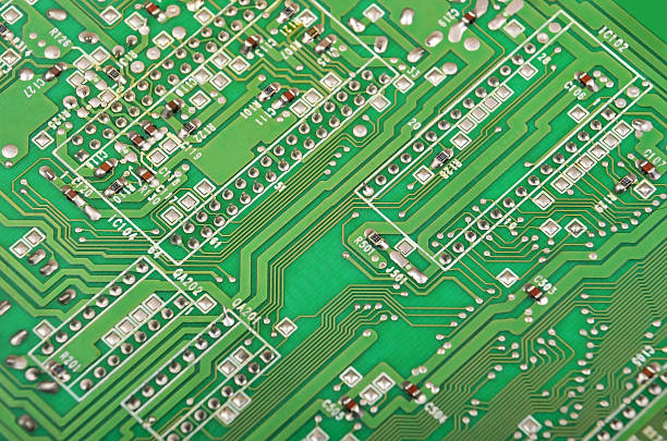
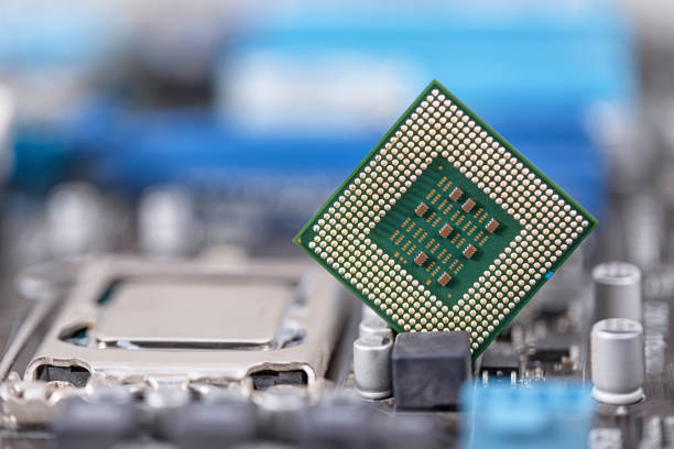
A thermal via is a plated through hole that connects the top and bottom layers of a PCB. In this way, heat is able to flow from the top layer’s components into the surrounding environment through the vias on the bottom layer. These vias can be filled with materials that enhance the thermal conductivity such as copper which are high thermal resistance conductive to manage the heat transfer efficacy. Designers may ensure maximal heat removal near heat generation parts via an array of thermal vias. In this way, the overheating effect can be eventually avoided.
Types of Thermal vias
Thermal vias have been grouped in several categories that describe the structure of these vias and the technology required for connection of shields from different layers within PCB. Here are the main types of thermal vias:
Through-Hole Vias
These are fully through PCB, hence, serving the connection of all the layers of the circuit board, from the top to the bottom. They are apt as heat conduction, but with large climber can absorb board space.
Blind Vias
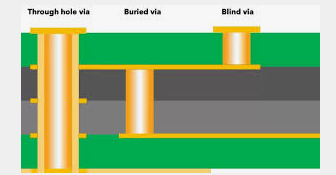
This is through-hole, i.e. the starting point of the connection is on an outer layer but the termination is in one of the inner layers. It is not necessary for them to fully pass through the board of the board. That way, they heat internal layers but do not affect the boards at all.
Buried Vias
Serving as a link solely with the CPU, these vias connect the internal layers but nothing outside. They are situated in invisible manner from the surface and the major application of these is to substitute for large number of multilayer PCBs.
Microvias
Lastly, we will look at the very small vias with a diameter rarely above the 0.15 mm, but mostly less than that, which are employed in high density interconnect (HDI) PCBs. They are either blind or buried and are more likely to be found in layers close to the surface where ventilation of the heat gain from high density components is improved.
Filled Vias
They are of any of the above types and combinations which are made of conductive or non-conductive materials that are used to increase thermal conductivity and mechanical stability.
Stacked Vias
This particular arrangement shall pin vias on each other that may have not been achieved without using all the trey layers. Consequently, the use of the stacked vias is prevalent in multilayer PCB to increase the thermal pad pathway
Staggered Vias
Lines look like vacuum arched vias, but completely different with normal stacking because they do not align one floor above another. Such relation assists in proper heating part of the puck and also the board’s general structural integrity.
Enhancing Heat Dissipation
Apart from making thermal vias that can take away heat from the critical components on your PCB, these structures also play an important role in that they reduce the ambient temperature holistically. Complements including CPUs, GPUs and amplifiers have thermal solder pad production by a conspicuous degree when they are used. The extreme temperatures of these components can be a threat to system performance if they do not properly dissipate heat, and as a result they might get damaged rapidly and components even fail horizontal thermal conduction.
Designers may take advantage of thermal vias in which they build a thermal interface material pathway for heat to exude from the components by including them in the PCB design. If you like this content, please feel free to share it. Vias can benefit in the intensity transfer from the component layer to the internal layers of the PCB and from there the heat can be escorted out to the surrounding ambiance. This results in the substrate’s temperatures being constant and prevents from lowering the device’s efficiency.
Improving Thermal Management
Thermal via also exerts a high impact on the improvement of thermal management mechanism on the circuit board. Through judicious positioning of thermal vias near the heat-generating parts, manufacturing engineers will be able to provide thermal paths for heat conduction that will not waste the heat output and cooling efficiency. This way, the component temperature gradient across the board will have a smaller range, so there will be no hotspots near the surface and isothermal distribution of temperature through the board.
Besides this, thermal vias can be fitted and coordinated with other techniques including those for heat sinks and thermal pads which optimizes removes low thermal resistance path energy improve heat dissipation. Hence, the thermal management system which is made of the integration of this all the approaches generally helps to boost the device reliability in the long run, especially in the extreme high temperatures.
How to Manage Thermal Vias and Placement in FR4
Managing thermal vias and placement in FR4 PCBs effectively involves several key strategies:
- Identify Heat Sources: Figuring out which high power components on your PCB cause major heating problems is a way to start.
- Use Thermal Vias: Put thermal vias in the proximity or underneath the individual vias that generate heat to ensure the transferred heat reaches the heat sink or any other cooling mechanism.
- Optimize Via Placement: Arrangement of Vias that contribute to the cooling of the expelled heat. Vias should be regularly distributed throughout and tightly located next to heating units.
- Increase Via Count and Density: More vias added means more paths for heat generated inward besides the decomposition.
- Select Via Size: Larger vias should be used to achieve better thermal performance considering it can take away more heat than the smaller I/O points might.
- Connect to Copper Planes: Be sure that the thermal vias are trace to the large copper pads, which serve as the thermal spreaders.
- Use Filled Vias: Keep in mind that non-conductive or conductive vias-fill materials are good for the getting heat insulated vias and better heat dissipation strength vias too.
- Thermal Interface Materials (TIM): Make use of thermal interface materials in between the component and the heat sink to boost heat conduction and remove heat more quickly.
- Simulation and Testing: Make use of thermal simulation software that helps analyze the distribution of heat and its optimum location to be utilized. Introduce the system into the real operational environment and check whether it is functionally efficient enough to handle heat management.
Sizing Thermal Vias for Maximizing Heat Transferring heat
When sizing thermal vias to maximize heat transfer on a PCB, consider the following factors:
- Via Diameter: A full flow that comes with the larger diameters provides a larger cross-sectional area and thus improves heat transfer. This would assure sufficient trading volume and liquidity, but then a diameter that is too big can result in the degradation of overall strength of the board. Normally, diameters go from 0.2 mm to 0.3 mm for which thermal vias can be made.
- Via Density: Numerous vias in the circuit help to increase the thermal transport. For an instance, having multiple vias spaced out and right below the heat dissipating components can make a good pathway for heat to spread laterally.
- Via Placement: Place vias right under or as close to the heat source instead of fain plantation cities, heavy traffic congestion, increased industrial output, violating air quality standards and comprising food quality are some of the consequences of increased copper layer thickness population. Make them a matrix using a grid or circular pattern within the area of a component.
- Pad Size: This crossing is well-controlled and the effective size of the pad on the top and bottom of the via must be adequate. Shaking the pad diameter to the elss, you will achieve better heat spreading but you can loose limited printed circuit board area.
- Via Fill: Incorporating thermally conductive paste (measured in terms of thermal conductivity) is an alternative to thermally non-conductive epoxy which has the advantage of better thermal transfer in the empty vias. Such an assembly has better thermal conductivity than air which results in its filling of crevices and air voids.
- Thermal Resistance: Evaluate the thermal resistance of the v-model to be able to compare it to other variations. Thermal resistances that offer lower values will have better heat transfers.
- Material Connection: Make sure to keep the vias well connected to the copper pad as well as to the inner copper plane which, in turn, function like heat spreading elements.
- Stack-Up Considerations: Via that goes through several layers in multilayer PCB create a hindrance to heat transfer as heat passes through. Employing vias in the vertically stacked and staggered pattern can be an effective way of moving the heat between layers which helps to keep the heat well spread.
- Software Simulation: Employ thermal analysis software suite to outline flow heat and to highlight possible hot areas along with efficiency of vias placement and the vias size.
Vias and proper via management
Effective via management in PCB design involves several key practices:
- Via Types: Smartly recognize the perfomance of various vias, namely through-hole, blind and buried, and select the particular one according to connections required on the board.
- Via Size: Electrical requirements often weigh in as a limiting factor, and the solution lies in the careful selection within sizes that adequately meet both performance and board area constraints. Pads that are bigger can have a larger current and sound more as heat.
- Via Placement: Create place to ensure routing the lengths of trace is as minimal and solve the signal integrity issues. In such places where tension develops, sound location can provide for improvement of technical resistance.
- Via Density: Add more vias into the high current lines in order to improve the current flow and to reduce the possibilities of the via failure. This may at the same time be effective in thermal management.
- Pad Size: Adjust the size of solder pads to eliminate the problem of shorting and thermomechanical stress during soldering while using the PCB area futilely.
- Stacked and Staggered Vias: Stack the vias for vertical connectivity across multilayer boards and stagger vias for the same so as to avoid misalignment during drilling. Create your own job Plans
- Via Filling: Use conductive or non-conductive epoxy to pour in vias to prevent solder in the assembly of a via in pads, which requires special attention if sig is to be ensured.
- Thermal Management: Apply the thermal via technique under components generating the most heat and distribute the heat evenly through the multilayered system by utilizing external heat sinks.
- Signal Integrity: In the case of high-speed or high-frequency applications, back drilled with via stubs to damp signal reflections and losses is required.
- Inspection and Testing: Fully comply with the inspections and testings procedures that are aimed at disqualifying vies that might cause problems or reduce reliability during PCB assembly.
Pad design for PCB thermal management
Effective pad design for PCB thermal management involves several considerations to enhance heat dissipation and ensure reliability:
- Pad Size: The pad size for component will be increased, Emphasis for the places that generate a large amount of heat. The increase of pad size allows for more heat dispersion over the PCB.
- Material: Use high-performing materials like copper for pads on the heat sinks for the effective transfer of heat from components to the board.
- Thermal Vias: Inlude thermal vias in the designed pad. These contact vias should be placed strategically targeting the hot components and offer heat conduction down to lower layers or heat-sink.
- Pad Layout: Make patches of these pads, with the surface area in closer contact to air achieved by natural cooling, or with the thermal interfaces enhanced heat conduction to cooling solutions.
- Solder Mask Exclusion: Decrease or eliminate solder mask for thermal pads which will help the thermal resistance reduction between the pad and the thick film resistor.
- Thermal Relief: Feature thermal relief pads for sensitive components that can become hot through soldering, this will permit normal temperature during soldering to prevent component or board damage.
- Simulation and Testing: Do the thermal simulation modelling, and perform the pad design optimization to reduce the cooling needs and power consumption. Prove the design with thermal testing under the full load operating the engine.
Thermal vias for heat dissipation in PCBs picture and formula
Thermal vias serve as a vitally important element of heat removal in PCBs, particularly, in high-powered as well as high-density electronic products. This is the short review of why heat vias act, as well as a simple formula for thermal dissipation calculation through thermal vias.
How Thermal Vias Work:
Thermal vias are small hole(s) in a PCB filled with or plated copper mainly which allows the movement of thermal heat between layers. These vias are sensibly spaced underneath heat-producing components to form a path for heat to flow from the highest layer, called package, where chip components are mounted, to lower layers or to the heat sink attached at the bottom of the PCB. Through this, the copper in vias gets to perform more efficiently in the heat transfer because it has higher conductivity than others.
Graphic Representation:
- Component Generating Heat: Being placed on the top the PCB.
- Thermal Vias: Small, plated-through holes that are placed precisely under the components.
- Heat Sink or Lower PCB Layers: It can be the destination either for bodies or for roads (the vias are heat exchancers).
The following is the graphic depicting a PCB with a thermal through hole. This visual depicts a bird’s-eye view of a PCB with a heat component in the middle, such as a microprocessor, emitting heat energy. A dwarf toroidal ring at the center of this chart is specified by a number of thermal vias of cruise and thermal vias which have no connection to an external layer or heat sink that is pictured with a shaded area on the bottom. This graph is aimed at being instructive presenting the importance of employing thermal vias in order to achieve a good heat dissipation.
Thermal vias structure
Heat thermal vias are a new generation of heat transfer pathways built into a PCB to facilitate the shifting of heat from power-consuming components to a heat sink or other dissipating systems. Their structure typically includes:
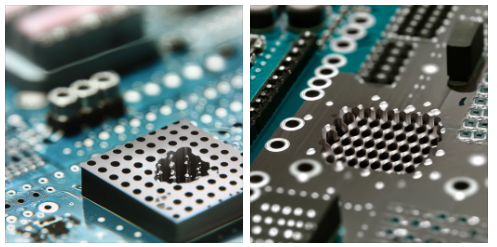
- Hole: A tiny opening drilled through one or more conductor layers of a PCB. It is common to be too small as it often measures less than 0.3 mm.
- Plating: On the walls whose thickness are made of a thermally conductive metal, which in most cases is copper, the heat passes more easily.
- Filling (Optional): At certain times, the vias may be filled with either connected epoxy to amplify heat transfer or with non-conductive epoxy as a structural supporter.
- Connection: The thermal via is then attached to copper foils or the heat distribution elements, which are in contact with the heat-generating compont on one side and heat sink or interface on the other side, to form a way for heat flow.
Benefits of thermal vias in PCBs
Thermal vias offer several benefits in PCB design, crucial for managing the heat in electronic devices:
- Enhanced Heat Dissipation: Thermal vias lead to the good transfer of heat from components with high temperature to heat sinks or other cooling fans layers. This way it is prevented from the hot up.
- Improved Component Performance: Through the decrease of thermals, the vias vapor pressure in the thermal vias allows for the electrical components to work under the ideal operating conditions, thus improving their performance and reliability.
- Increased Device Longevity: Dissipation of heat is accompanied by the elimination of thermal effect on the functional materials, thus the life expectancy of the device will increase.
- Enables Compact Designs: Predominantly, the better temperature management makes closer placing of components without the worry of the heat interference. As a result, it is possible to have more compact and efficient PCB layout.
- Higher Power Density: Such components make the panels hotter reducing the optical power levels at the photodetector.
- Reduces Thermal Hot Spots: The concern of hot spot formation can be resolved with symmetrically placed thermal vias. Hence, it would lead to other heat zones which are responsible for more uniform heat distribution.
- Cost-Effective: Utilizing the thermal vias is an efficient and convenience way of overheating of PCBs maintenance without spending a lot.
Conclusion
Thermal vias are a must-have element in PCB design, with their role being crucial not only in high-temperature applications but also in those where heat dissipation is a major issue. By making thermal vias, which dissipate heat, around heat-generating components, such as power amplifiers for radio applications, the designers are able to increase the heat dissipation and manage the overall thermal performance level of the PCB. Thus, it keeps the right running temperatures, stops the device from overheating, and results in undeviating operation of the electronic products.