This comprehensive reference, from the basics of vias to the application of advanced routing techniques, discusses how to make your PCB designs both functional and performant. One of the key focuses of this session will be on diodes, their types, placement strategies, and impedance considerations. Through this, you will learn to navigate and eventually confidently tackle all the layers and complexities of design.
What is Via?
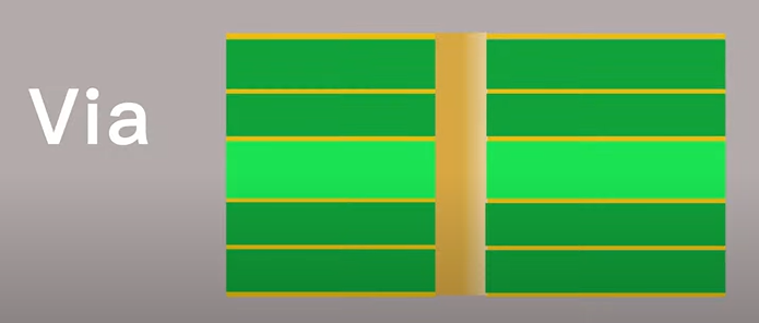
A via, which is an abbreviation for “vertical interconnect access,” is a principal element in the PCB. or This conduction connection is like the links in the vibration chairs that electric signals travel through. It is able to pass the electric signals from internal layer to different layers. Through-board vias are normally small holes drilled through the surface layers of PCB substrate holding metal (commonly copper) plating for the purpose of electrical interconnections between the inner layer. For these reasons, they are invaluable in wiring the electrical signals together between components, power planes and PCB’s copper traces, making the creation of complicated yet compact electronic systems possible. Via types include through-hole vias (PTH) and surface mount vias (SMT), each of which is meant to meet the relevant design specifications and the PCB manufacturing environment.
What is the Purpose of Via in PCB?
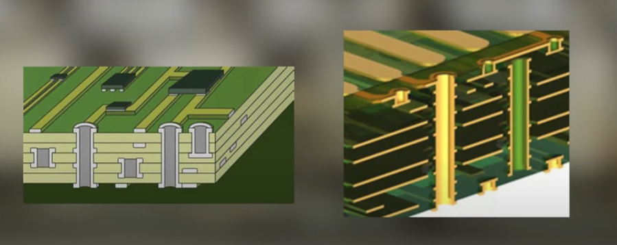
The role of vias in a printed circuit board (PCB) is to establish the junctions between the board layers and to generate the electrical connections within the PCB. Vias constitute the links or transmission of signals of power and ground between one layer and another via in pad design; thus, through the inter-connectivity mechanical connection of the different traces, electronic components are able to communicate and interact across multiple layers of the PCB. Here are some key purposes and functions of vias in PCBs:
- Signal Routing: The traces are routed to both layers of the PCB to connect the signals from one PCB component to another and vice versa, completing the entire connection on the circuit board.
- Power and Ground Distribution: However, Vias are the elements of the PCB used to connect power and ground plane on different PCB layers, thus guaranteeing the integrity of the design and the stability of operation.
- Component Interconnection: Vias secure a way for the components to be connected together on different PCB layers of the board. This way, it becomes possible to make the electronic assemblies rather compact with a dense layout of components.
- High-Speed Signaling: In high-speed digital and RF circuits, vias are very important component which helps to keep signal integrity good enough by preventing reflections, mismatches and discontinuities.
- Thermal Management: Vias act not only as structural and electrical functions but can also perform heat dissipation activities as heat from components or thermal pads of one layer can be diffused to another layer with heat sink or thermal plates, thereby helping in the temperature regulation of entire PCB.
Types of Vias in Printed Circuit Boards
These are the types of PCB vias:
Through-Hole Vias (THVs)
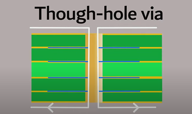
Through-Hole Vias (THVs) constitute an indispensable element in PCBs. They play a critical role in establishing electronic communication between separate electronic layers. THVs are well-known for the bore they make that cuts through hole components of the entire PC board substrate, from the top to the top and bottom layers together.
Blind Vias

Blind vias is a particular type of via required in printed circuit boards (PCB) used for the connection between the surface layers on the outside and one or more inner through vias without the necessity of passing through the whole thickness of the board. On the contrary to via-saal ho vias (by means of which it is possible to get through the PCB), the blind vias have only a certain depth, and they end at one of the internal PCB layers.
Buried Vias
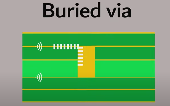
Vias that are located inside printed circuit boards (PCBs) are a type of via that is used as inter-layer connection without penetrating the outer layer of the PCB. In contrast to through-hole vias, which pass through the whole thickness of PCB, buried vias remain within the core layers and are barely visible from the outer surface of the board.
Microvias
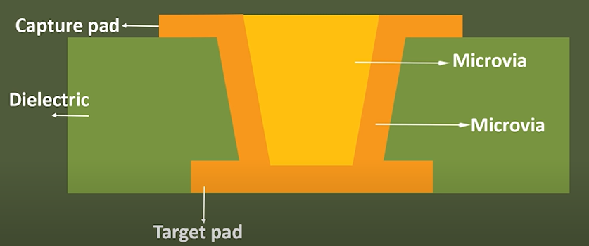
Microvias are the smallest standard pinholes used in printed circuit boards (PCBs) to allow the passage of electric lines across different PCB layers of the board applications in high-density interconnect (HDI) PCBs.
Via-in-Pad (VIP)
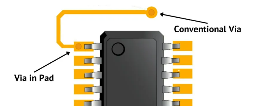
Via-in-Pad is a design technique known as VIP that integrates a via within a component pad on the PCB. With pins located between component pads, vias can encumber available PCB space, hence electrode routing.
Filled Vias
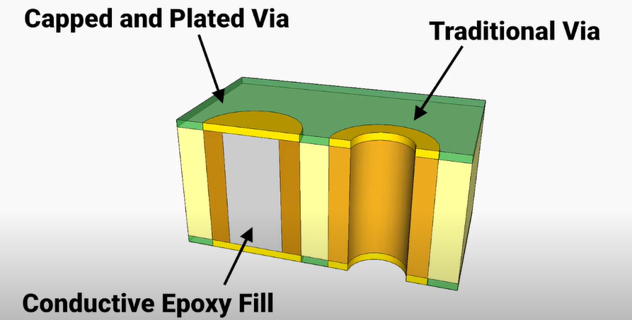
The filled vias, likewise referred to as plated or fully thermal vias or filled-through vias, are the most commonly used kind of via in machine-to-machine communications or printed circuit boards (PCBs), where, after being laser drilled, the whole via hole is plated through holes and filled with a conductive path or non-conductive material. There are two primary types of filled vias:
- Conductive Filled Vias
- With the conductive-filled vias, performance of drilled hole is improved by filling it with conductive materials like solder mask, solder paste or conductive epoxy after drilling.
- This material works as an electrical continuity conductor that allows passing electricity between different layers of the PCB. At the same time, this material strengthens the via.
- Conductive-filled (or filled) vias, providing an extended route for current flow and a greater degree of conductivity, are most commonly found in applications where high mechanical strength and current flow are critical.
- Non-Conductive Filled Vias
- Vias contain of non-conductive material that can either be filled with epoxy resin or non-conductive material after drilling.
- The non-conducting characteristic of the material greatly strengthens and supports the via structure, preventing air and moisture from getting trapped, hence delivering reliable PCB.
- Non-conductive holes filler vias are among the electrical insulation and paths of the environment, conducive of many applications.
Capped Vias
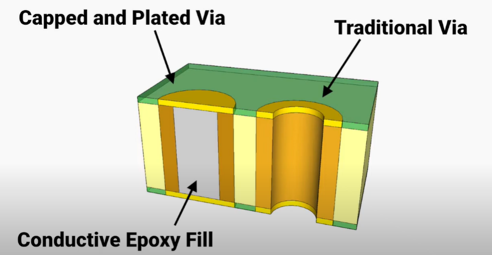
Capped vias are a reference type in PCBs where the via opening is covered by means of other material, usually non-conducting, to close down the via. There are two primary types of capped vias:
- Non-Conductive Capped Vias
- Non-conductive capped vias are well sealed by a layer of non-conductive materials such as epoxy resin or solder mask.
- The capping is made of a non-conductive material whose purpose is to close the opening formed by the via. This protection is against environmental factors and keeps foreign substances out of the creation.
- Such vias are normally employed in the high-reliability versions where electromagnetic interference, arc-over and contamination with atmosphere are critical.
- Conductive Capped Vias
- Conductive and capped interconnections, covered with solder, are generally designated as type V via.
- conductive cap, on the one hand, acts like a plug but also continue the electrical connection for multiple layers of PCB.
- Supply the conductive-capped vias when you have to pay attention on both the electrical conductivity and the way against environmental features.
How to Determine the Right Via Requirements for your PCB
Deciding the ideal via parameters for your PCB project necessitates taking into account several determining factors to obtain a board with the best performance, reliability, and manufacturability. Here are steps to help you determine the appropriate via specifications for your PCB:
- Understand the Design Requirements
- Enumerate the layout design particulars you want to know, including the number of layers, signal integrity constraints, routing density and component positioning constraints.
- Evaluate Signal Integrity Needs
- Before starting, know the signal integrity requirements of the layout design, such as the speed of the signal, matching impedance, and line transmission aspects.
- Consider High-Speed Design Guidelines
- Please adhere to high-speed design guidelines such as controlled impedance routing, avoiding signal reflections, and signal stubs if your design involves high-speed signals (for example, DDR memory interfaces or high-speed data buses).
- Assess Layer Stackup and Routing Density
- Review your PCB stacked vias layout and give some thought to the number of signal layers, power plans, and ground planes which affect signal connection. Decide on the best via forms (these include through-hole, blind or buried vias) and their placement so that they allow for the routing of signals without any issues and control signal integrity and impedance variations.
- Select Appropriate Via Types
- Identify the suitable via styles to meet the particular requirements of your printed circuit board design. In this case, the author emphasizes the importance of making the right choices during the layout design process, considering the particular requirements. An examples, through-hole vias will work best for general-purpose connections, whereas blind and buried vias will be very useful for more dense designs where routing space is limited .
- Consider Manufacturing Constraints
- Consider the PCB manufacturing constraints, like whether the PCBA can be fabricated or not and meeting the cost requirements to enable the manufacture of the product. Validate that your PCB comprises the proper via types and specifications that support the capabilities of your PCB fabricator.
- Evaluate Environmental Factors
- Think of the environmental factors, including temperature variations, humidity and vibration, that could affect the performance of your PCB. Select options, such as materials and specifications, that can endure the required service conditions and provide high dependability in operation.
- Perform Design Reviews and Simulations
- Review the designed PCB board for the main issue of routing tools and properties of vias, and the verification of PCB design requires the application of PCB design software simulators to support performance and reliability specifications.
Adjacent layers in PCB Via
Vias are used to make electrical connections between the layers of the board parallel to the printed circuit board (PCB). When the ritual is set up, it becomes able to view signals, power or ground that are transferred between the adjacent circuit layers. So, the PCB vias allows traces or components on different layer to be connected. Here’s how vias between adjacent layers in a PCB work:
- Drilling: At the very start, the geometrical structures of the vias are being drilled with the help of this placing method. These holes generally allow penetration of fibrous epoxy resin laminates through the thickness of the PCB substrate.
- Plating: The subsequent procedure involves the creation of perpendicular walls into the via holes, followed by the deposition of any conductive material (typically copper) on to the hole surfaces. The whole plating plot serves this plan’s purpose.
- Interconnection: After the via plating, they ensure signal transmission (or power and ground signals), which allow for vertical connection among adjacent layers of PCB. The multilayer board design establishes an easy operation of component connecting, and it is the most effective method for wiring traces of different planes, which gives the PCB the capacity to function as a single electronic circuit.
- Routing and Layout: In the PCB layout process, engineers plan the placement of vias to show up an interconnection (between layer traces) in order to get satisfactory signal integrity, routing density, and thermal management. The positing and clicking PCB vias are a function of the particular needs of the printed circuit board and also of the suitable performance of the circuit.
Why is a Via to Internal Layers marked as 1–16?
The term “1-16” means the numbering and naming method that we use to name or label the PCB vias that are used to connect the outside or outer layers of the printed circuit board (PCB) to internal layers. Here’s what each part of the notation represents:
- “1”: This means that the start or origin of the way is marked by it. Following such a number, “1,” implies that the routes being described begin from the top layer of the PCB or towards the bottom of the PCB (Layer 16). The number “1” specifies the first layer, whereas “16” represents the last layer if there are no more layers. Assuming a typical two-sided PCB, where layer numbering is from top to bottom, “1” stands for the topmost layer, while “16” is the bottom layer.
- “16”: This signifies that via is indicating either the destination or target layer. This implies “16” as an interior layer end point of the PCB. 16 would be interpreted as Layer 16, or the bottom layer (with the top layer as Layer 1). Inside layers are known as I, II, III, and so on. The lower the number, the deeper the tier within the PCB system.
Conclusion
Vias in printed circuit boards (PCBs) are critical elements that provide the means for a perfect coincidence of electrical connections among various circuit layers. Thru-holes, or vias in PCB design, perform two roles. First, they facilitate signal, power, and ground paths between layers by penetrating the PCB substrate. Second, they can be used as interconnecting components and traces in multilayer PCB designs. Besides being utilized as connection points between the outer and inner layers, vias are also stairways to provide the vertical routes in a printed circuit board, which are the necessary parameters to realize the function, performance, and reliability of the electronic devices.

