Get to know the backdrilling of PCB inside out with our ultimate guide. From getting into the basics to the latest strategies, take a deep dive into backdrilling for the best printed circuit board layouts. Uncover the process sequentially, explore its advantages, and determine the correct guidelines to boost your PCB designs with respect to accuracy and rationality. Refine your skills and transform your style of the back-drilling process, starting immediately.
What is PCB Back Drilling?
Back drilling, or controlled-depth drilling, is a method used in PCB (Printed Circuit Board) production to trim excess cutting via drill holes that can be damaging impedance, especially in high-speed digital networks and RF (Radio Frequency) applications.
Why is back-drilling required?
The purpose of back drilling in PCB fabrication is to meet several requirements concerning signal integrity, most of which come up in digital and RF (radio frequency) circuits. Key reasons why back drilling is necessary:
1. Reducing Signal Reflections
This causes the relevant section of the stub to act like a transmission line discontinuity and hence a reflection of the signal occurs. These reflections often alter the shape of the signal and thus lead to many timing errors in high-speed digital circuits. The process of back drilling removes the sidewall stubs that are the source of signal reflections and allows the signal to flow to its destination.
2. Minimizing Crosstalk
As for vias with long stubs, they can become a source of unwanted crosstalk recorded from adjacent signal traces or layers. This is the result of the electromagnetic fields of one signal getting involved with the others, causing disturbance. Back-drilling vias are considerably shortened, minimizing cross-talk possibilities.
3. Maintaining Impedance Matching
In fast circuits, there is a need to preserve impedance matching in order to have clear signals. The excess length of stray stubs will lead to the change of the transmission line characteristic impedance, thus impedance mismatching. impedance of signal paths is kept constant by turn drilling that removes the disconnector stubs.
4. Improving Signal Integrity in RF Circuits
The RF circuits are dependent on higher frequencies, where any impurities or disruptions to the signals yield substantial effects on performance. Back drilling is an important process when designing RF PCBs so that the signal integrity of radio frequency signals can be preserved and degradations reduced.
5. Meeting Design Specifications
These modern electronics include data centers, telecommunication equipment and high-performance computing systems, such that signal integrity specifications must be followed rigorously. Frequently, back drilling must be done to achieve this requirement, and the device’s operation becomes reliable.
6. Enhancing High-Speed Data Transmission
Practically, led hole drilling has been key in improving these high-speed serial interfaces, such as PCIE (Peripheral Component Interconnect Express) and USB (Universal Serial Bus), among others, thanks to the increasing need for bandwidth.
Advantages of Back drilling process
- Improved Signal Integrity: Back drilling as a method of reduction of via stub lengths decreases signal reflections, thus signal distortion minimization is undertaken. This consequently results in enhanced signal integrity to ensure that the signals propagate somewhat through the PCB without much degradation, especially in the high-speed digital and RF circuits.
- Reduced Crosstalk: The shortening of long stubs through back drilling contributes to the disconnection of adjacently placed traces or layers, thus lessening the coupling influence and cross-talk. This is key to the proper functioning of the signal and its segregation, especially in multilayer printed circuit boards.
- Enhanced High-Frequency Performance: In RF and high-speed digital circuits, it is very critical to reproduce constant impedance and least signal distortion, which are the key requirements for high-frequency reliable performance. Back drilling serves this purpose by filling in the interruption in chain lines and immobilizing impedances.
- Compliance with Design Specifications: A large number of electronic systems, well known by telecommunications, data centers, and high-performance computing, have that very strictly determined signal integrity requirement. Back drilling enables designers to meet their required specifications since it is the only way they can keep the signal paths conforming to the desired impedance profiles and without any signal reflections.
- Optimized PCB Layout: Back drilling enables PCB designers to create more compact and efficient layouts by reducing the required clearance around vias. This allows for tighter routing and placement of components, leading to higher-density PCB designs without sacrificing signal integrity.
- Enhanced Reliability: Back drilling allows for minimizing the signal distortions and gives the possibility for stable signal propagation. By doing so, the electronic system is more reliably working. It acts as a barrier from signal errors, timing problems as well as data corruption as a result comes a better robustness and durability of the assembly of PCB.
- Compatibility with High-Speed Interfaces: Backdrilling is therefore crucial for achieving the cohesion of high-speed parallel interfaces such as PCIe, USB, SATA and Ethernet. This is why back drilling complements them, as it combines low-jitter signal reflection and stable impedance characteristics.
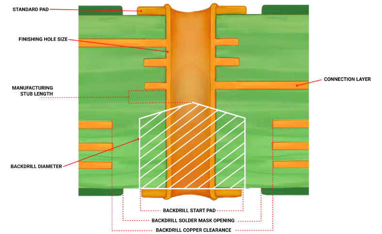
Back-drilling Design Values
To develop PCB back drilling, both signal integrity and manufacturability need to be considered, as they best ensures optimal PCB routing and signals. A good PCB re-drilling designer has deep knowledge and skills on how to be able to complete the back drilling with the best possible way to ensure signal integrity and manufacturability goals are met with minimum costs incurred.
- Drill Depth: The drill depth calls for an exit point from the back drill in which the desired amount of via’s length is discarded. Depending on the PCB stackup, it is usually set by the board design and desired end point of the multilayer PCB. An appropriate drill depth control is needed to avoid damage to the sensitive layer or the nearby trace layer that is the signal carrier.
- Minimum Drill Diameter: The minimum drill diameter limit determines the size of the drill bit, which will have a smaller diameter than the minimum drill diameter limit. This value characterizes the via size, along with the necessary gap between the via and other constituent elements of the printed circuit board.
- Annular Ring: The annular ring is the copper ring which surrounds the hole after drilling. More than one back-drill to maintain the integrity of the annulus (electrical connection & mechanical stability) is mandatory.
- Back Drilling Tolerance: Back drilling tolerance is the deviation fortified by the diameter and depth of the drilling. Critical constraints can be found in the process of keeping the tolerance tight in order to obtain consistency in the signal processing and to avoid any signal degradation.
- Stack up Considerations: The PCB stackup involving the count and placement of layers affects the back-drill-down value of impedance. The different stackup architectures might need to be fine-tuned in terms of hole depths and sizes for the purpose of eliminating vulnerabilities from signal integrity across the board.
- Signal Integrity Constraints: Differential pairs and high-speed serial signals within the back-drilled holes that are specified for the PCB design should have their signal integrity kept in mind during the back-drilling design process. The limitations that need to be confronted include matching impedance, propagation delays, the limitations of signal reflection, and crosstalk.
- Manufacturing Capabilities: The back drilling design values can be dimensioned to suit the capabilities of the PCB assembler as the equipment for drilling is available. Motors just make-do with drill depth, diameter, and tolerances based on a manufacturer’s equipment and processes.
- Cost Considerations: The selection of back drilling design values should also take into account social implications of production costs. Strict tolerances and complex processes of drilling will drive up cost of manufacturing so it’s crucial to find a balance between performance requirements and effectiveness.
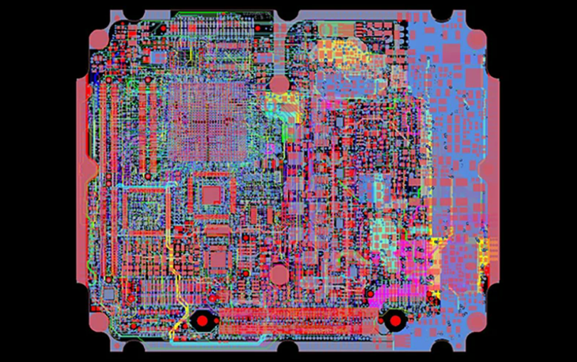
Backdrilling PCB technology
Backdrilling technology in printed circuit board manufacturing exactly cuts off material from via stub lengths and blind vias, improving signal integrity in high-speed and RF circuits by getting rid of signal reflections, crosstalk, and impedance matches. By using advanced CNC drilling machines, the drill layer pair column depth and diameter can be precisely adjusted to only eliminate the signal parts that are more excessive than others without changing the signal layer, retaining signal integrity. By closely cooperating with PCB designers, the PCB board manufacturer comes up with the backend process specification that best suits its production competency and efficacy; this, in turn, brings down overall cost. On-going seeking for the best way and optimization, backdrilling plays a key role in the electronic industry to achieve quality results that can work in various types of applications.
Back-drilling PCB DFM tip
At the DFM phase, back drilling fits in; therefore, it is vital to work closely with the manufacturers. Through early commitment, designers would be in a position to adjust the back drill diameter specifications for depth and diameter to suit machining capabilities, as well as ensure efficient alignment with the requirements of the supply chain, thereby maintaining the probability of avoiding scheduling mistakes. Besides the mentioned DFM analysis tools , designers should aim to examine backdrilling compatibility as well, and on their part, they should try to solve the composition issues when first identified. This policy is ensured by methodical documentation and meticulous verification, which negates the likelihood of degrading data transfer. Coming from the prototyping stage to iteratively upgrading the manufacturing process based on business partner’s feedback is a roadmap for optimizing the process and boosting the efficiency and quality of PCBs.
Backdrilling PCBs from a manufacturing perspective
The backdrilling performed by a PCB manufacturer is a vital measure to elevate signal integrity, especially when it comes to high-speed profiles. It deals with the exact amount of deposition through the via or through-hole by utilizing the information gathered in design process. The already-drilled hole is extended and subsequently formed by editing the drilling file to indicate the backdrilling depth. Thus, precision equipment is next mounted to perfectly bore the removed material to the adjacent layers of the copper barrel. Preceding anywhere we dream, rigorous inspection and quality assurance are performed to check the precision and regulatory desire. Tracking and recording the procedures involved in backdrilling can be an important piece of evidence and a valuable reference for future use. When done, the backdrilled PCB may go on to the decisive stage of mounting the respective components. In this way, the performance and reliability of the final product are guaranteed.
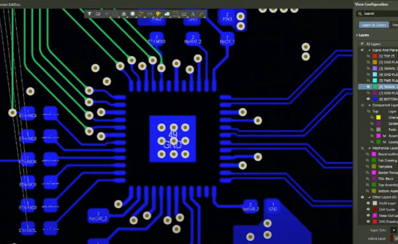
Controlled Depth Drilling from a Design Perspective
Application of controlled depth drilling in printed circuit boards covers two different aspects: signal integrity and structural integrity or signal layer usage results. Specialists come up with a detailed position of certain holes that have to be made to the accuracy of the drilling depth, comprising of overall technical specifications. They do PCB layout revisions based on manufacturability and signal integrity considerations. They take into account RxD and TxD capacitances and bus speed so that it can work properly according to the sample code. This method provides less distortion in the signal and this is the reason for flawless data transmission in high-speed modules. Accuracy in manufacturing is the other antithesis environment and a good collaboration with manufacturers requires the ability to ensure proper application during the manufacturing process. In reality, controlled-depth drilling does increase both the electrical and mechanical conductivity of the PCB.
Advantages of back-drilling PCB PTH vias
Back-drilling PCB plated-through (PTH) vias offers several advantages, particularly in high-speed and high-frequency circuit designs:
- Improved Signal Integrity: This process secures better reliability of the connectors as it provides continuous connection between the layers and reduces signal reflections and impedance variations. This is of paramount importance in hi-speed digital and RF circuits for the same eventuality because these degradations of signals lead to data transmission problems.
- Reduced Stub Effect: Through the process of back drilling, the stub effect created by the undersized components extending beyond the predetermined signal layers are removed. Stubs are equivalent to impedance mismatches and distortions of signals, whereas physically removing excessive material has, as a result, bringing about the elimination of such.
- Minimized Crosstalk: Back drilling minimizes crosstalk interferences between adjacent lines by destroying raised vias that would otherwise propagate along the layers. This will help continue the signal isolation and the probability of interference is lowered, especially in lines with clutter due to the densely populated PCBs.
- Optimized High-Frequency Performance: The anti-drilling is effective in microwave and RF devices so it minimizes signal losses and impedance discontinuity, thus ensuring accurate signal propagation and working at high frequencies.
- Enhanced Manufacturing Yield: Back drilling has a better check on two main causes: short discontinuities and excess vias material that is beyond the stated layer thickness or required target layer thickness. Consequently, to achieve better PCB fabrication, there is need for high-quality PCBs and fewer manufacturing defects.
- Increased Design Flexibility: Through back-drilling process, designers can have more controlled profiling, thus enhancing the flexibility of the Routing high-speed signals. This practically demonstrates how little PCB space is needed with complex layout concepts.
- Compatibility with Multilayer PCBs: Back drilling can be used in multilayer PCBs consisting of a stack of vias, enabling for consistent signal integrity between multiple signal layers. This is necessary to get rid of disturbances of signals that are approaching each other in multiple, dense signal layers of printed circuit board (PCB) layout.
Primarily, throughput of PTH vias back drilling in PCBs has a lot of merits, including better signal transmission and integrity, reduced interference by absorbing excess current on the board, and a high manufacturing yield, hence the good technique suggested in modern high-speed design circuit designs.
Signal Attenuation in Back-Drilling
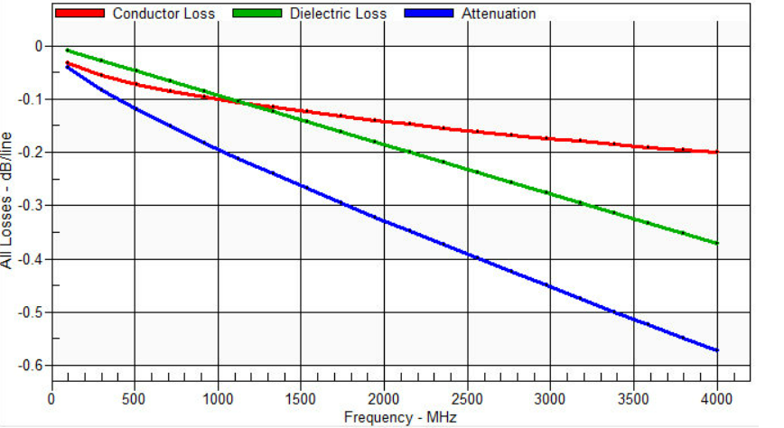
In back drilling, the fading of the signal strength or amplitude is the attenuation, which is one of the disadvantages of PCB manufacturing with minimum and maximum variations. While back drilling is primarily implemented to improve signal integrity by reducing impedance variations and signal reflections, it can introduce some level of signal distortion issue attenuation due to various factors:
- Material Removal: By back drilling, the process includes the removal of the excess materials in vias or through-holes, thus lowering the area of cross-section conducting the path. This will decrease conductive material and, therefore, result in high resistance, then finally signal attenuation.
- Dielectric Losses: The presence of dielectric that happens to be surrounding the conductive tracks emanating from the PCB can also cause signal loss in some case. Partial drilling may cause changes in the substrate’s dielectric properties; hence, we may notice higher dielectric losses, especially at higher frequencies.
- Transition Regions: Transition parts from the back-drilled portion (unused portion) the via and the unaffected part can result in considerable signal discontinuities. Blocking may give rise to impedance mismatches and reflection with the number of times the signal is attenuated, depending on the number of transitions.
- Length of Back-Drilled Region: The back-drilled region elongation leads to its signals weakening. Although the back-drilled high-resistance impedance may seem higher than expected, it can be further increased by making the back-drilled region longer, which can lead to higher attenuation due to additional resistance and dielectric losses along the signal path.
- Frequency Dependency: The magnitude of radio signals in back drilling is significantly frequency-dependent. High-frequency signals will suffer more due to the attenuation effects caused by the larger dielectric and impedance values in controlled-depth drilling.
To sum up, PCB back drilling is a vital process of modern PCB manufacture which contributes a lot to enhancement of signal quality and suppression if interference. Although this problem of signal attenuation might arise, back drilling carried out perfectly can help with such issues, and the extra steps of impedance matching will ensure the absence of this issue. Via and through-hole back drilling take place after the material is trimmed back into the drilled hole. It minimizes signal reflections, impedance variations, and crosstalk by precisely eliminating the excess material. Thus, the reliability of high-speed and high-frequency applications is ensured. On a whole, PCB back drilling is a procedure that adds to quality, efficacy and dependability of electronic circuits, which is a basic tool in modern PCB design and manufacture.
Conclusion
In conclusion, PCB back drilling is a crucial technique in modern circuit board manufacturing, offering significant benefits in improving signal integrity and reducing interference. While concerns about signal attenuation exist, meticulous execution of the back drilling process and complementary strategies like impedance matching help mitigate any potential drawbacks. By precisely removing excess material from vias and through-holes, back drilling minimizes signal reflections, impedance variations, and crosstalk, ensuring reliable performance in high-speed and high-frequency applications. Overall, PCB back drilling enhances the quality, efficiency, and reliability of electronic circuits, making it an indispensable tool for modern PCB design and manufacturing.