Delve into the PCB assembly universe with this comprehensive guide that starts from rudimentary concepts to advanced methods. No matter if you are a beginner or a seasoned guru in PCB assembly, this comprehensive tool is the ultimate thing you need to know to assemble PCB like a pro. Consider basic topics including component selection, soldering techniques, PCB layout design, and solving typical issues. The guide will provide you with a comprehensive step-by-step assembly process, useful practical suggestions, and insightful visualizations that will guarantee that you will successfully master wiring your first printed wiring board and be able to unleash your creativity in electronic designs.
WHAT IS A PRINTED CIRCUIT BOARD ASSEMBLY (PCBA)?
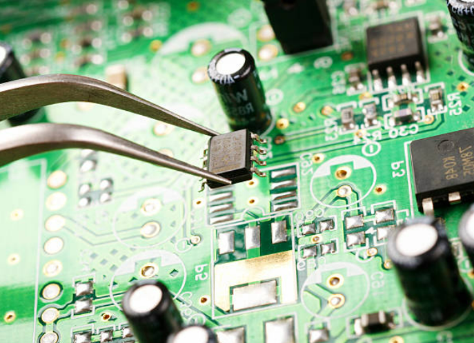
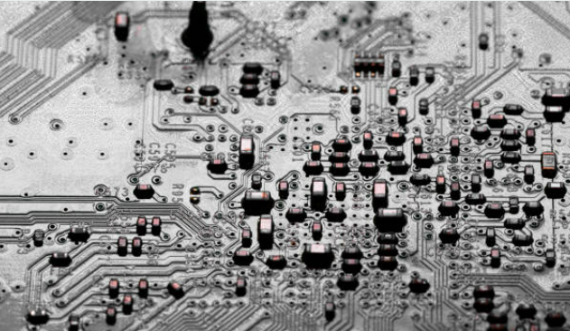
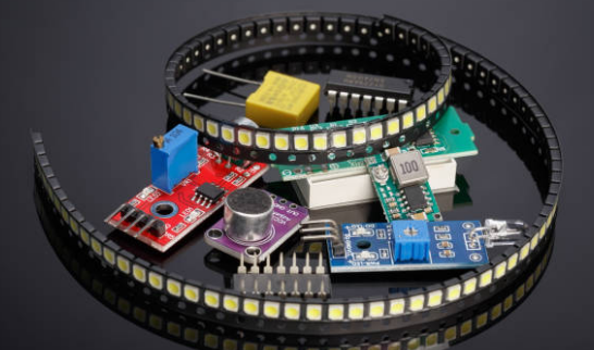
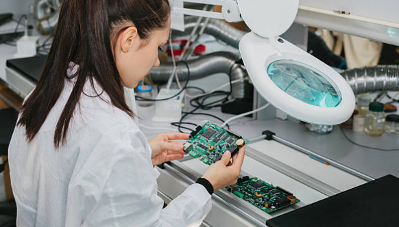
PCB assembly (PCBA) is the process of mounting electronic components on a PCB surface to make a fully operative electronic device. These parts, which are resistors, capacitors, and integrated circuits, as well as connectors, are picked and mounted onto the PCB in accordance with the design of the circuit. After it attach components, they are welded to the PCB using techniques like wave soldering, reflow soldering, or manual soldering in order to form electrical interconnections. After the assembly process of the circuit is done, it undergoes final inspection to check whether all the components of the electricity system have been placed correctly and soldered together properly. Further, these steps of functional and in-circuit test conduction are carried out in order to verify the functionality and performance. PCB assembly could also be tested for conformal coating or encapsulation, which will protect the assembly from environmental factors. PCBA plays a significant role in guaranteeing that electronic gadgets match up with quality specifications in their functioning as well as in producing devices that are durable and reliable for the intended application.
TYPES OF PCB ASSEMBLY
These are the types of PCB assemblies:
Through-Hole Assembly (THA)
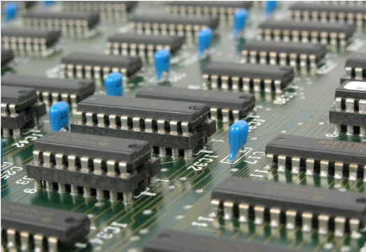
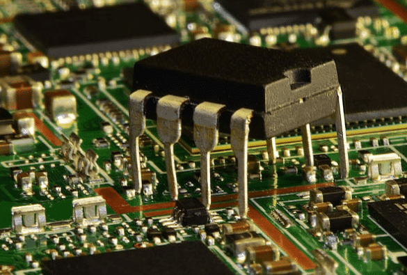
The Through-Hole Assembly (THA) is a technique in electronic circuit board mounting process in which the components’ leads or pins are inserted through the holes drilled into the board for the components to stand upright on the assembled board. Unlike SMT assembly, which transfers components directly onto the PCB board surface, THA goes through the underside of the board to solder component leads to their respective pads on the opposite side. The THA has been a traditional approach for multiple reasons, including the requirement of stronger connections or in the manufacture of low-volume assemblies. Parts were designed and manufactured with the THA due to its benefits over other assembly technologies Nevertheless, THA does retain significance where misplaced components that are meant for surface mounting are unsuitable, such as those that require more strength for mechanical purposes, and continuation with THA remains popular in aerospace and automotive companies due to their resilience and ease of inspection.
Surface Mount Technology (SMT)
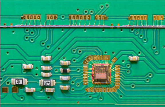
Nowadays, Surface Mount Technology (SMT) assembly is usually used for electronic circuit board assembly, whereas in through-hole assembly (THA), holes in the circuit board are previously drilled and components are soldered onto the circuit boards. In surface-mount technology, components are fastened to the board by the leads that would roll onto the top of the board, and then accessories are attached to pads that are the same size as the leads. Generally speaking, these assembly processes are operated by pick-and-place devices that move each component into the appropriate site determined by layout. SMT assembly has the following advantages over THA: high component density, smaller board size, and improved electrical performance due to the engineers of short signal path. It is currently one of the most broadly utilized techniques in modern industrial production of electronics for its productivity, competitive advantages, and adaption to miniaturization and large-scale manufacturing.
Mixed Technology Assembly
Mixed Technology Assembly combines Through-Hole Assembly (THA) and Surface Mount Technology (SMT) assembly onto the same printed circuit board (PCB), resulting from the increasing number of electronic devices that incorporate both types of assembly. The advantage of this technique is that it can use either surface mount or through-hole components in a single printed circuit board assembly, so that the strengths of the two types of technologies are combined. The most apparent advantage of through-hole components across the board is their solderable leads, which provide a robust mechanical connection liable to meet the needs of components with higher power handling or mechanical strength. Meanwhile, the surface mount components offer advantages in size, weight, and cost-effectiveness, among other measurable aspects. The mixed assembly technique is often applied in situations where a number of different components are used to cause a specific type of behavior or function or to achieve a given performance level, giving an option for different design and manufacturing.
Single-Sided Assembly
The single-sided assembly, however, is an instance of a circuit board manufacturing process in which only one side of PCB is being populated with electronic components. The construction, which incorporates components by either through-hole components or innovative SMT assembly approaches, is mainly dependent on the specific project requirements. The single-sided board assembly technique is often employed in those uses where the size of the printed circuit boards is not an issue and the application space is not a major concern. It enables economies in production through single-side PCB manufacturing without the complexity of a double-sided or multiple copper layers. Meanwhile, though, it will reduce the packed density of part elements on the panel and will not be an ideal choice for more fixed electronic layouts.
Double-Sided Assembly
Double-Sided Mounting, on the other hand, is a way of constructing electronic devices in which components are assembled on both front and reverse sides of the printed circuit board (PCB). Using this method, a more component-dense assembly and a greater fidelity of circuit designs can be achieved as compared to single-sided printed passive bare board assembly. In double-sided construction, parts could be mounted using both the through-hole assembly technique and the mount mount technique. The parts could then be placed according to preference and availability. This strategy is most commonly employed when place efficiency is important or if highly complex circuits are required where components are placed on both sides of the PCB. Double-sided assembly requires a lot more care and can also be challenging and time-consuming as compared to single-sided assembly due to the need for accurate and in-time component placement for soldering on both sides of the board. On the flip side, it opens new design possibilities and provides the platform to manufacture all the necessary electronic devices and applications as well.
Multi-Layer Assembly
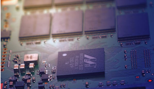
The advanced Multi-Layer Assembly (MLA) method is a modern production technique that enables the creation of PCBs with more than two conduction layers separated by the insulating material. Through the extensions of linings, these layers can make contact through vias that will be useful for circuit designs with high component density and good signal quality. Multi-layer PCBs are a primary component in electronic devices that have little space for expansion and require high processing power, e.g., computers and smartphones. The completion of this assembly process is done using this method. It involves placement and precision alignment of layers, drilling of vias, plating with non-conductive substrate material, and lamination. The mounting of elements using these options, including whole assembly (THA) and mounting on the surface (SMT) technologies, offers a range of choices in design and functionalities. Despite seeming to be more complicated, the multi-layer process is basically an inherent property of modern electronic circuitry since it endows improved design flexibility, electrical performance, and reliability.
Step-by-Step Process in the Assembly of PCB
The PCB assembly process usually contains multiple steps, which start with the design of a circuit pattern and end with the examination and visual inspection (or testing) of the completed board. Here are the step-by-step process in PCB Assembly:
Design and Layout: Information engineers create PCB circuits that carry out special synthesis utilities considering signal routing, component placement, and thermal management, among others. They are responsible for ensuring the design of the product will comply with electrical and mechanical requirements, including EMC and signal integrity concerns.
Manufacturing the PCB: The very first step of the PCB assembly process is formatting the substrate material, which is usually FR-4-type epoxy laminate. The photolithography technique is utilized for the purpose of transferring the circuit layout onto the substrate, which is carried out by revealing the semiconductor via a process of being exposed to light through a mask, followed by chemical etching, which is used for the removal of unwanted copper traces.
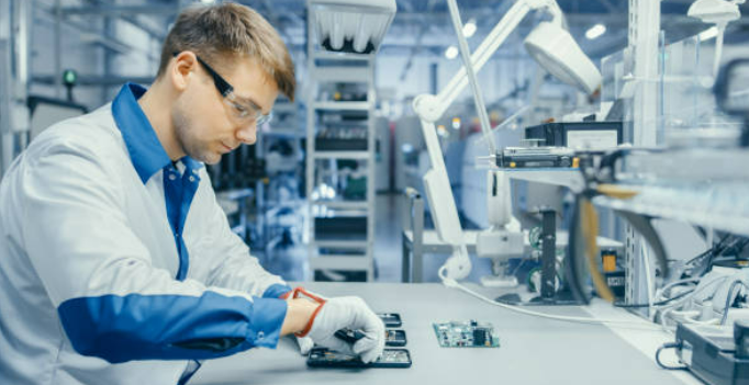
Component Procurement: Purchasing specialists identify the components from the known suppliers and check for other goods that are of good quality and authentic. These items perform functions such as hindering components from deviating away from the limits set by the selection of bill of materials (BOM) in relation to tolerances, ratings, and package sizes.
Stenciling: A pre-formed stainless steel stencil made up to the overall PCB design pattern is placed over the board. Next, the board is screened from the front by means of applying solder paste, which is a mixture of solder mask particles and flux used to create an exact solder paste deposit on each pad area.
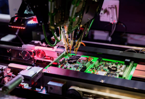
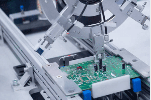
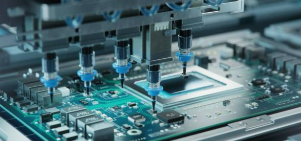
Component Placement: Robots do the same job as humans, with the PCB files guiding each robot to place components on the board at high speed. Such equipment can automatically position components accurately based on the vision system to the required tolerances.
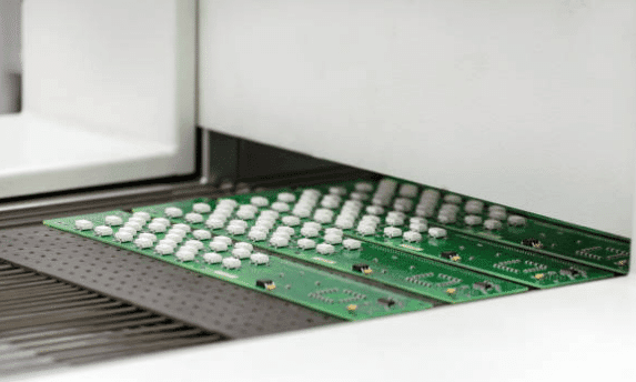
Reflow Soldering: The reflow process in the oven then takes the PCB, which is now fully populated with components and solder paste. The precise temperature of the oven ensures the gradual heating of the board. While the soldering paste is melted, the solder joints between the components and PCB pads are formed and shaped into a solid state.
Through-Hole Component Insertion: Through holes are either drilled by hand or with automated insertion equipment to hold the components in the PCB. PCB leads are then cut to length, and the traces on the board will undergo soldering during the final PCB assembly process stage.
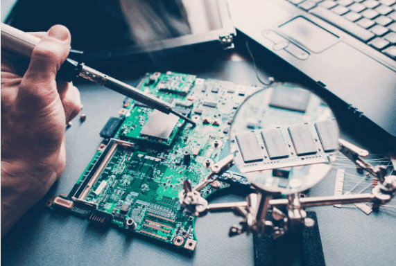
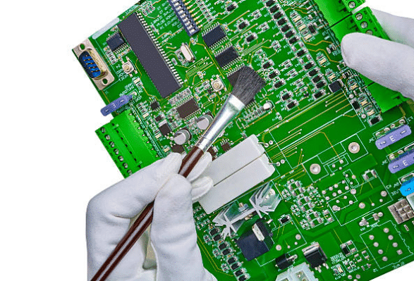
Cleaning: After successfully soldering the PCB, it goes through cleaning to get rid of flux residues and other contaminants. Generally, cleaning is done thoroughly so as to prevent contamination of any parts that may affect the PCB’s reliability and lifespan.
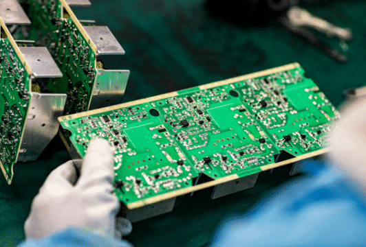
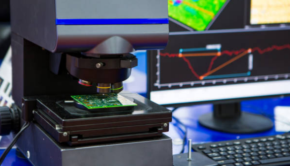
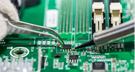
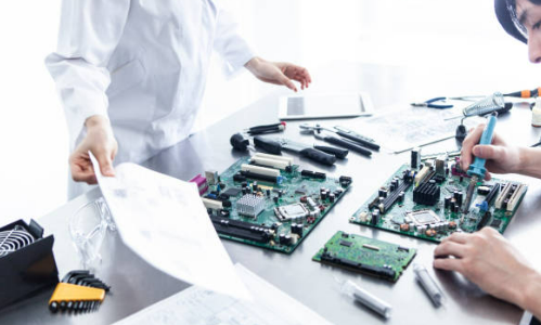
Inspection: The assembled PCB then goes through a rigorous quality control process involving checking from defects and errors through the various stages. Visual optical inspection (AOI) techniques and X-ray machines that facilitate the detection of faults like mispositioning, disparities or absence of components are used.
Testing and Quality Control: The manufactured PCB then goes through a tough battery of tests to attest to its functionality and general excellence. This can be accomplished by using electrical testing with the help of automated test equipment (ATE). It can also carry out boundary and short/open checks by a functional test to find out that the PCB operates the way it is expected.
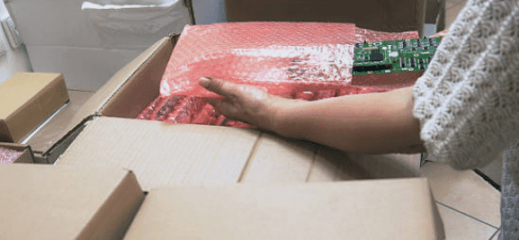
Final Packaging: After performing tests and quality control checks, the PCB is finalized for engineering. Consequently, the PCB producers could apply protective coatings, stamp them with serial numbers or barcodes, and pack them anti-statically for shipments to the customers.
Documentation: Meticulous monitoring is undertaken at every point within the manufacturing system and all steps are recorded in order to maintain traceability. For the PCB record, relevant data traces are recorded, such as component sourcing records, assembly instructions, test results, and any changes made during the PCB process. This creates a chronological record of the manufacturing of the PCB.
Importance of Automatic Optical Inspection in PCB Assembly Process
Automated optical inspection (AOI) is a crucial element of PCBA; it provides the needed fault detection and electronic device reliability during the manufacturing process.
Here’s why Automatic Optical Inspection (AOI) is important:
- Accuracy: These systems deploy state-of-the-art cameras and algorithms offering unparalleled accuracy, with finesses in spotting deformities such as misaligning, missing items, bad soldering, or incorrect polarity.
- Efficiency: Automatic Optical Inspection is an automated inspection system, and hence it is able to streamline the inspection procedures and reduce the associated time and resource consumption. Being flexible is not only about efficacy but also speed in production cycles, which result in quicker production cycles. Consequently, turnaround times are shortened.
- Cost-effectiveness: Automatic optical inspection decreases the chance of human error and detects defective products early in the production process, thus preventing costly rework as well as scrap. Introducing AOI technology to an enterprise eventually might save its costs because it decreases waste and raises the general level of quality of the goods.
- Reliability: Automatic optical inspection allows manufacturers to ensure standards of quality consistency on a par with products in the industry and meet customer needs. This dependability is vital in general but is especially important for those industry sectors where PCB failure is not an option, such as aerospace, automotive, and medical devices.
- Process Optimization: The Automatic Optical Inspection method helps the manufacturer obtain invaluable data relating to the manufacturing process, and the analysis of such information by the manufacturer enables him to recognize patterns and faults to be rectified and implement some corrective actions. It is the recurrent cycle of improvement that adds to the increased process efficiency and the higher quality of the product to catch up in time.
PRINTED CIRCUIT BOARD ASSEMBLY STANDARDS
PCBA standards develop consistency, quality, and dependability all the time during the manufacturing process. Some widely recognized standards in the industry include:
IPC-A-610
The standard IPC-A-610, approved by the associated industry group of IPC, dictates the acceptability of electronic devices and other connected assemblies, including PCB assemblies. It touches upon areas like solder paste soldering, component mounting, dirtiness, surface finishes, and inspection criteria, which delivers whole information for quality control and inspection across the series process.
IPC-J-STD-001
This standard defines the soldering norms applicable for soldering processes that are utilized in the manufacture of electronic assemblies. It includes soldering materials, tools, techniques, and inspection of soldering joints, as well as soldering electronic components via through-hole, surface mount, and cable connections. IPC-J-STD-001 implements further ESD guidelines as well for demagnetization of both charged components and materials.
IPC/WHMA-A-620
The IPC/WHMA-A-620 standard calls for the setting up of requirements and acceptance standards of wire harnesses and cable assemblies manufacturing. It deals with factors of materials, assembly, crimping, soldering, examinations, and inspecting criteria for wire harnesses in order to guarantee that they manufacture them uniformly and reliably.
ISO 9001
Although it is independent of PBC assembly, ISO 9001 is an international standard frequently used for quality assurance, especially in other industries. It is highlighting customer services, continuous enhancements, and its guided path towards creating QMS within the firms. ISO 9001 certification has proven a company’s dedication to quality and customer satisfaction that exceeds expectations in any phase of the PCB production process.
ISO 13485
The standard is all about quality management system for medical device industry that set requirements to achieve safe and effective device. Together with the mechanical and electrical aspects of medical devices, it lays down a standardized approach for assembling the PCB used in medical devices, ensuring compliance with regulatory requirements. This, as a consequence, will keep the products safe and efficient. The ISO 13485 certification basically serves to certify organizations involved in the manufacture of medical PCB assemblies. The assertion is quite paramount, seeing as company endeavors and initiatives need to be in line with the specified regulatory requirements of the healthcare sector.
UL 796
UL 796 is the safety standard for boards with a printed circuit. This standard is mandatory for components used in devices or appliances, when applicable. It specifies what is required from materials, construction, performance and testing to ensure that the boards are up to standard and safe enough to use. The conformity of PCB assembly with the UL 796 standard is a guarantee of their ability to meet the extremely severe security requirements and can be applied in consumer electronics and industrial gadgets.
RoHS Directive (2011/65/EU)
The Restriction of Hazardous Substances (RoHS) directive restricts the use of hazardous materials like lead, mercury, and cadmium and a variety of other substances contained in electrical and electronic equipment, including PCB assemblies. While RoHS compliance necessitates lessening the hazardous materials used in PCB assembly practices, it also introduces safety to the environment and people’s health and promotes sustainable manufacturing practices. Compliance with RoHS directive is a legal necessity in many countries, regions and territories around the planet, which include EU-certified or approved products by testing and certification.
Full-turnkey printed Printed boards
PCB manufacturing in the full turnkey version involves a set of services offered by PCB fabrication and assembly firms, which makes them responsible for almost the entire process, from pick and place machines to the finish of assembled boards. What is special here is that the manufacturer is taking care of the whole process, from sourcing components to the assembly and testing of their PCB boards, which guarantees their customers a complete solution. Here’s how the process typically works:
1. Design Consultation
Through the first meeting, the team of the manufacturer may make suggestions about design perfection, materials use, and cost-effectiveness issues. They involve the client in the process and help them understand their goal better by introducing a dedicated phase of product requirements collection and goal determination. This ensures that the end product is exactly what they need.
2. PCB Design
Engineers at manufacturer’s use advanced software tools to design a PCB layout that takes care of things like signal integrity, thermal management, and manufacturability. They may have digital modeling and simulations to facilitate design optimization for the purposes of functionality and durability.
3. Component Sourcing
The manufacturer holds connections with a number of high-quality component suppliers and distributors; thus, the manufacturer impresses the brand image with the quality of the parts assembled through the process. They inspect suppliers and certify that some are in accordance with industry standards and regulations to avoid using products or PCB assembly services that are not authentic.
4. PCB Fabrication
The fabrication process is carried out in keeping with quality standards, and the use of new equipment contributes to the production of high-quality products. Highly sophisticated methods like laser drilling as well as quality control of impedance matching are called for in order to satisfy individual requirements of the given design.
5. Component Assembly
They control the assembly process according to a strict schedule, and besides, they have automatic optical inspection to make sure the components are in the right place and aligned correctly on the printed circuit boards. Automatic optical inspection machine systems, which are automated optical inspections, may be used to check component placements and ensure that no errors or defects have been detected.
6. Soldering
The solder joint-forming process is regarded as a crucial stage in soldering and is being monitored for consistency and reliability. Using sophisticated soldering approaches as well as selective soldering, vapor phase, and reflow soldering, the manufacturing industry could achieve high soldering quality while there is a minimum possibility of defects being observed.
7. Testing and Quality Control
Along with functional testing, manufacturers also do environmental testing to determine the behavior of the PCBs under different conditions like temperature, humidity, and vibration. Here, the understanding is gained that the PCBs conform properly with the dimension and standardization for the intended applications.
8. Final Packaging and Delivery
The manufacturer implements special packaging solutions that safeguard the PCBs during transportation and storage. They might have available options for bulk packaging, tray packaging, or custom packaging, depending on the preferences of clients and shipping needs.
9. Documentation and Support
Full documentation is furnished with each lot of PCBs, consisting of current certificates of compliance, test reports, and governing documentation records. Of course, manufacturers, aside from the delivery, continue to provide support to address any issues and inquiries that are post-delivery in nature, thus ensuring a seal of satisfaction and confidence in the product.
Customers can go through a complex process with PCB manufacturers in a full turnkey solution, where they will benefit from the same services such as quality, consistency, and reliability, right from the design to the delivery. Such a prototype is more convenient to pick and place machine use for those customers who don’t possess the needed expertise or resources to work with multiple suppliers and for customers who cannot agree to cooperate on various aspects of the PCB manufacturing process.
Conclusion
To wrap it up, the assembly of printed circuit boards (PCBs) is a pivotal process in the electronics industry, in which electronic components are placed on the printed circuit boards to form the desired website circuits. From the perspective of THA as well as the SMT board PCB assembly process, many different things need to be kept in mind, such as component placement, soldering methodology, and industry standards, to ensure the performance and reliability of the assembled printed circuit board. Through collaboration with well-known PCB assembly companies as well as employing advanced manufacturing techniques, companies could manufacture PCBAs that conform to their individualized demands and are instrumental in the production of their electronic products.