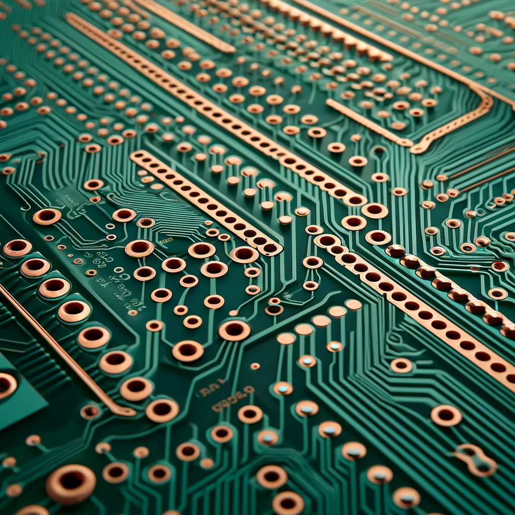
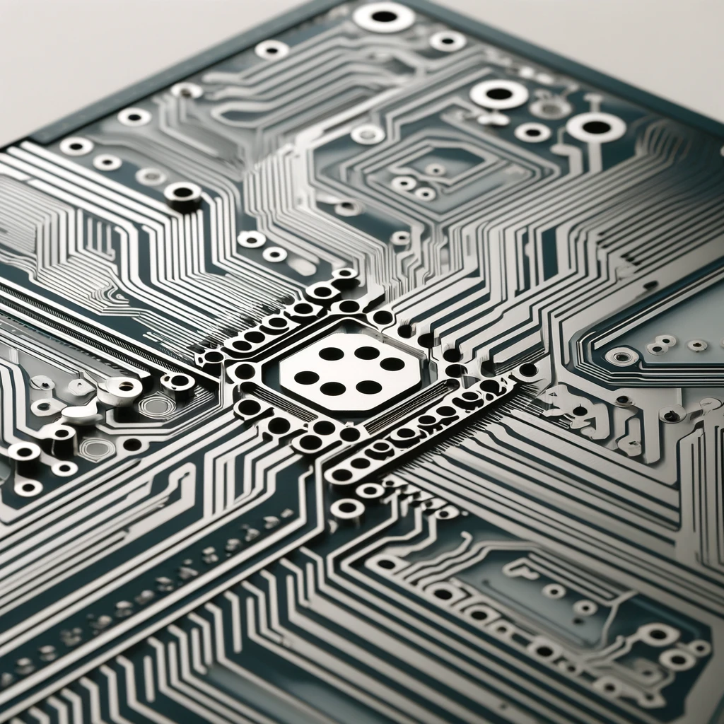
In PCB design, the passing of conductors from the top through to the bottom surface necessitates the use of many vias. However, this may have negative implications when it comes to the board’s performance and space. In addition to other types of vias, blind vias and buried vias are the ones that play a key role in modern PCBs, especially with the devices becoming smaller and more complex.
The content revolves around why blind vias get attention, the benefits they offer, the manufacturing process, and how they are used in PCB design.
What are blind via?
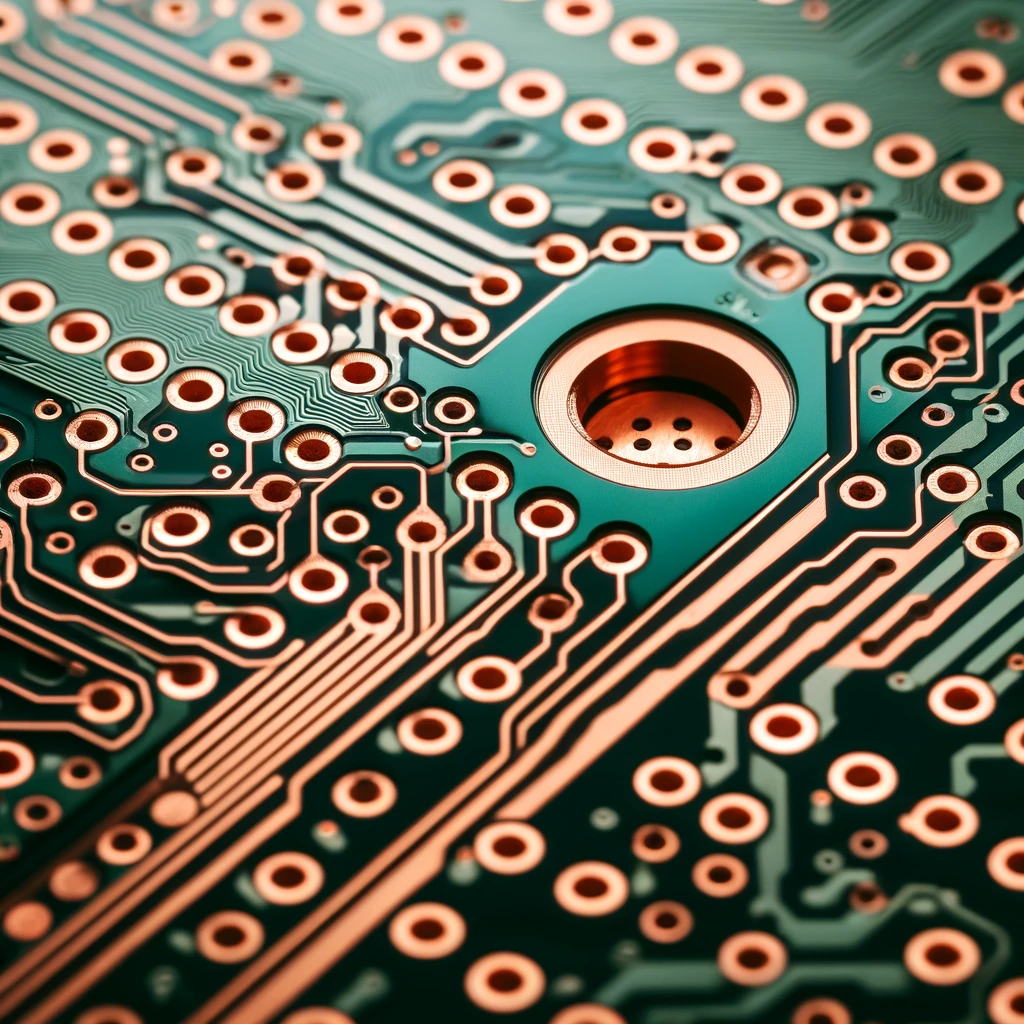
Blind via is the term used in PCBs to connect the outer layers to one or more inner layers without going through the whole board. These vias stay imperceptible on the opposite side of the circuit, and hence they are known as “blind.”. Such types of vias are a valuable asset for designers who want to minimize space utilization of aspect ratio and upgrade the performance of multi-layer PCB boards into the outer layer.
The Benefits of Using Blind Vias
These are the benefits of using the Blind via:
- Space Efficiency: Blind vias also reduce the board area because they do not have to be vias that penetrate through the entire board, thus, the design become more compact.
- Improved Signal Integrity: Using Blind Via-place signals do not have to travel long distance, which helps improve performance in GHz frequency applications.
- Enhanced Thermal Management: They do the job of a heat conductor, i.e., heat generated from heat source components is transferred systematically to heat sinks or outer layers, which helps to enhance thermal management.
- Increased Design Flexibility: Blind vias allow the number of layers on the PCBs to be increased without changing the board size, thus enabling the fabrication of more complex circuits.
What are the potential problems with blind vias?
Potential problems with blind vias include:
- Increased Cost: Manufacturing blind vias is usually more costly because of the specialized processes used in those processes.
- Complexity in Design: The board designers have to pay special attention to the planning of the PCBs in such a way that everything goes smoothly in this phase, but this can be a problem.
- Reliability Issues: If the use of blind vias is not properly conceived, the through-connections between layers will be less reliable, and the performance of the PCB will be affected.
- Inspection and Repair Difficulties: Blind vias are not easy to inspect and fix because they are not visible through the entire board.
- Limited Availability: Not all PCB manufacturers who are capable of achieving high-quality blind vias are available in the market, making the market pool smaller and thereby the options to source limited.
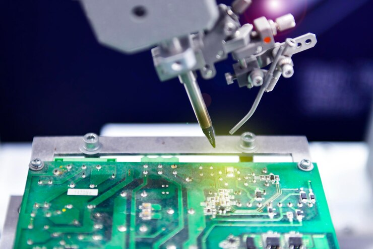
Manufacturing Techniques
The production of blind vias can be done using various methods, the choice of which depends on the specific requirements of the PCB and the manufacturing facility’s capabilities. Common techniques include:
Mechanical Drilling
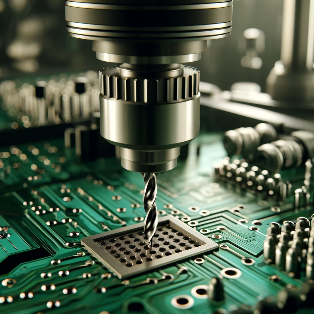
Tailored traditional drilling methods where the via is not very small keep the costs down at the same time. This approach is worthy of praise as the monetary cost of the device may be lower, but in return, the complexity of the device decreases, especially in high-density boards.
Laser Drilling
For the blind vias to be more refined and accurate, laser drilling is often used. It offers the opportunity to build such slender vias, down to the size needed for the HDI circuitry.
Photo-defined Vias
This method is based on the application of photolithographic processes in order to identify the slot while imaging, which gives the possibility of exact placement and precise size engineering.
Applications in PCB Design in blind via
Blind vias are highly beneficial in scenarios where space and speed are the main concerns. Some common applications include:
Smartphones and Tablets: These devices necessitate implanting, space-fixed, yet highly focal PCBs, playing with the immense number of functions that make area efficiency maximization a sine qua non.
Wearable Technology: Gadgets including smartwatches and fitness trackers reap the advantages of blind vias that go along with their space-saving uniqueness.

High-speed Computing: Blind vias are used on servers and computers that have to handle high-speed data transfer to improve signal integrity and reduce noise.
Challenges and Considerations
While blind vias offer numerous advantages, they also present certain challenges:
- Increased Cost: The production process for blind vias, particularly laser drilling, can be a significant contributor to the cost of the PCB.
- Design Complexity: Incorporation of the blind vias requires fantasy and care to prevent durability and manufacturability problems.
- Repair and Inspection Difficulties: The reason for that is that, as a result of the non-establishment of the throughput line, they are rather difficult to inspect and fix when they develop problems.
Advantages of using blind vias
Advantages of using blind vias include:
- Space Efficiency: They save space on the printed circuit boards by not penetrating all layers, allowing for more compact designs.
- Improved Signal Integrity: Shorter via paths can reduce signal degradation and improve performance.
- Enhanced Thermal Management: Provide direct heat paths to outer layers, improving cooling.
- Increased Layer Density: Enable more circuit layers without enlarging the Printed circuit board size, ideal for complex electronics.
- Aesthetic Cleanliness: Keep the opposite side of the board clean, which can be beneficial for both functionality and aesthetics.
Blind via manufacturing considerations
Considerations for manufacturing blind vias like controlled depth blind vias include:
- Cost: These procedures are usually more expensive as usually ultrasounds and drilling machines have a specific setting.
- Design Complexity: The design and layout of the layout must be very precise and right in order to ensure the correct placement and functionality.
- Equipment Capability: Encouraging precision is a starting point for any drilling procedure, be it mechanical drilling or an imaging study demonstrating the site.
- Material Considerations: It is very important to choose a suitable substrate and copper thickness that will not adversely affect the survival of this through-hole during and even after the fabrication process.
- Production Yield: The complexity of the process increases, which can lead to a decrease in output if the process is not well managed.
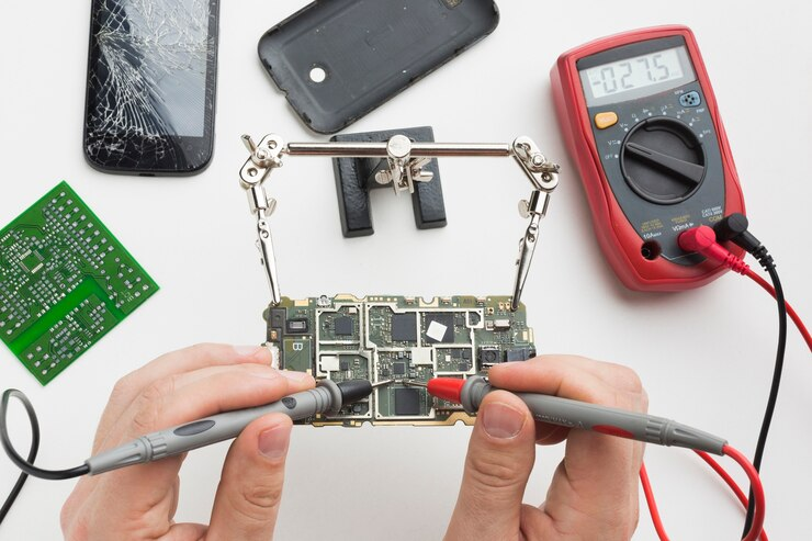
- Testing and Inspection: Allows cameras to inspect and test large area via holes, blind and buried vias, which are not fully visible from all sides and, therefore, require the special inspection methods.
Conclusion
Blind vias are a key element of contemporary PCB design, which makes electronic devices more efficient, compact, and high-performance. Learning about how to engineer good power delivery for different applications becomes an important factor in delivering the highest possible function for any electronic product. As technology innovates even further, the significance of creating blind vias is all but certain to further expand, giving extra leg room to electronic design.