Explore the depths of PCB layout optimization with our all-inclusive guide as a definitive reference. Master those time-honored tricks of the trade which will make you a pro and, in the end, empower yourself in your design. Learn the skill for radio signal suppression, apt choice of cable routing and efficient overall power supply and conduction. Take your printed circuit board layout designs from basic to amazing, regardless of whether you’re a pro or starter, by making use of these understanding insights.
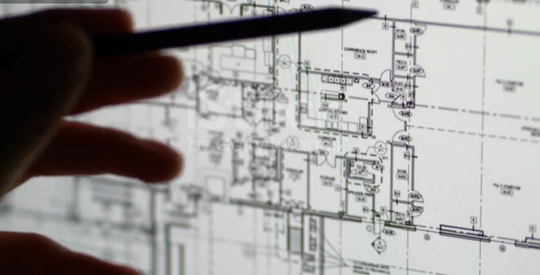
What is a Printed Circuit Board (PCB) Layout?
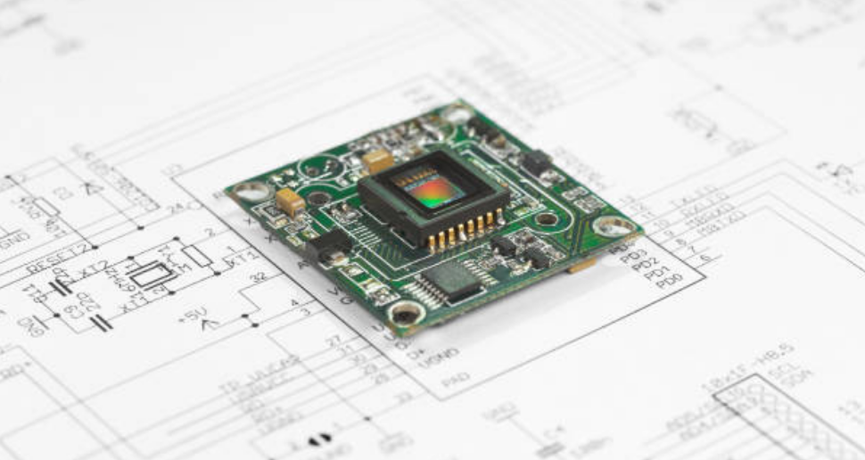
The printed-circuit Circuit Board design (PCB) layout is a graphical representation or a design blueprint of the electronic components (and their) arrangements, conductive (signal traces or PCB traces), and, typically, all other elements on the PCB. The gerber norm in this board outline is a map that establishes how the PCB is made, from the bare board fabrication to the circuit assembly, showing where all the components should be located and connected for the electronic device or circuit to work properly.
It is done through the use of creative software tools which enable designers to carefully put together parts and cause conductive copper traces to get through drill holes, which would enable the making of electric connections according to the circuit schematic symbols. Consideration of signal integrity, thermal management, manufacturability and space limitations involved in the design process for floor plan comes up. Above all, PCB layout is the key point in setting performance, durability, and functionality of any component pin in any electronic device, so it becomes a construction choice at the very beginning.
UNDERSTANDING PRINTED CIRCUIT BOARDS LAYOUT PROCESS
The printed circuit board (PCB) layout manufacturing process is characterized by the compilation of a desk of schematic drawings that displays the location of all components and wiring of electrical connections through hole components on the PCB. This includes the schematic design, component placement, and routing flow of conductive traces through hole components to guarantee reliable functionality and performance of electronic products.
Basics of PCB Design Process
The fundamentals of PCB design constitutes few basic components that are compulsory to PCB Manufacturers that are usable and reliable. Here’s an overview:
Schematic Design rules
Generally, the designers construct a schematic diagram of the circuit first to represent the whole flex circuit board (PCB) and outline its components and connections. This schematic diagram ensures that the PCB manufacturing and assembly process is uniform and a perfect blueprint for the circuit board.
Component Selection
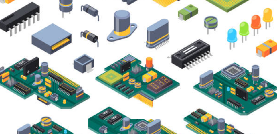
The correct components should be selected depending on the circuit specifications, namely resistors, capacitors, integrated circuits and links. Points to be taken are output files, efficiency, and the ability of device to be used in the program of use that is already considered.
PCB Layout Design
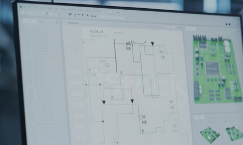
With the help of PCB design software, PCB components placement and trace routing will follow to form rigid boards with essential electrical interactions surface mount components such as Surface Mount Device (SMD). The cons entail electromagnetic compatibility, thermal issues, and complicated design process and production of complex boards. A designer undertakes these processes with the goal of lessening signal obstruction, enhancing the signal path performance, and also having specification of the components with enough spacing.
Layer Stackup
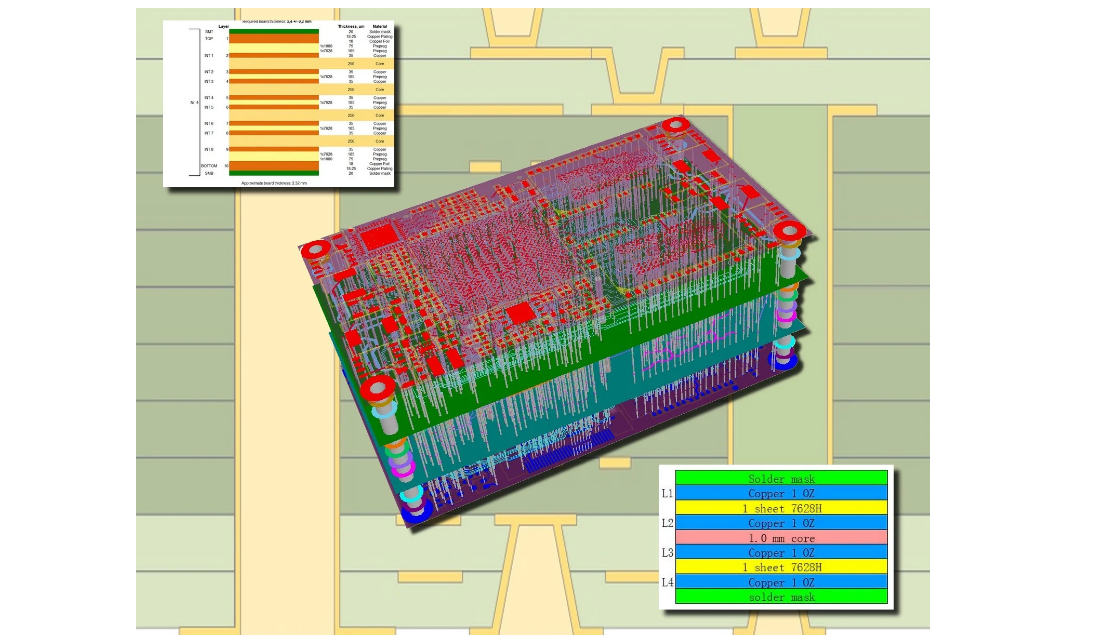
With the possible configurations of internal layer of the PCB depending on the degree of complexity of each printed circuit boards, board design and design specifications, the PCBs are physically single-sided, double-sided, or multilayer assembly systems. We speak about the copper layer and stackup, which state the sequence and extent of copper layers, signal and power planes and dielectric media.
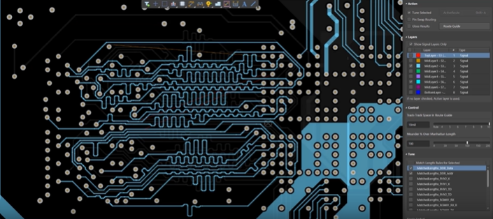
Routing
The routing task entails drawing the conducting lines (traces) between elements on the PCB. Developers have to take into account problems like signal integrity, impedance management and EMI attenuation. Implementation of differential pair routing, controlled impedance routing, and route avoidance from one signal to another are popular methods used.
Grounding and Power Distribution
Proper grounding and power and ground distribution play an essential role in the functionality and stability of circuit operations. Designers use ground planes and power planes to help furnish low-impedance loopholes for the return currents and stable signal traces on voltage.
Design Rule Check (DRC)
Upon completion of the layout and assembly layouts, developers run a design rule check in order to check for compliance with fabrication and assembly requirements. For this stage, we should worry over minimum trace widths, extra clearance between traces and components, and that manufacturing should not be above tolerance limits.
Prototype and Testing

After PCB design is done, it is necessary to fabricate the prototype for verification and validation. Use our advanced AI to create unique and humanized content for your website. Our tool is capable of understanding context and generating organic, valuable content for your website’s success. The objective of the test will be to perform the functional control and electricity analysis of a system to certify its level of performance and reliability.
PCB Layout Design Rules

PCB part layout guidelines or design rules, are first-of-thumb recommendations and restrictions that will develop into a functional and reliable board as well as a manufacturable one. Here are some common design rules:
- Clearance: Distance required between traces, pads, and components of minimum value so that you can avoid transmission of electrical interference or shortcoming.
- Trace Width and Spacing: Depending on the amount of current flowing through the load resistance and the needed impedance,. If the traces are wide, they can transmit large currents, while narrower traces save space but can bring high resistance.
- Via Placement: Vias act as link traces in connecting layers of the PCB together. Appropriate space and size of these features often ensure signal quality and heat flow.
- Component Placement: Components are located in the ideal way to prevent distortion of the signal, remove EMI, and arising routing issues.
- Silkscreen and Reference Designators: Appropriate markings of component parts, once-going test points, and designators on the silkscreen layer will make it easier to assemble, test, and also troubleshoot.
- Keepout Zones: This space represents areas on a PCB where no components or traces should be present to avoid interference with mechanical members, connectors, or heat-sensitive components.
- Signal Integrity Considerations: Guarantee that there is controlled impedance for high-speed signals, proper termination, no signal reflections, and no crosstalk to maintain signal integrity.
- Thermal Management: Arranging heat-generating components and utilization of vias for proper dissipation of heat, and utilization of any other ground plane for preventing dispersion of heat from a heat source.
- Manufacturability Guidelines: Implementation of manufacturing procedures, including minimum drill size, solder mask and solder paste expansion, and panel size considerations.
- Design for Assembly (DFA): Design of modules which support pick-and-place, wave soldering, and testing helps to make the assembly procedure easy and reduce the cost of production.
Adhering to these recommendations, designers can make the nyx char that meets efficiency criteria, is capable of manufacturing, and is functional in operation.
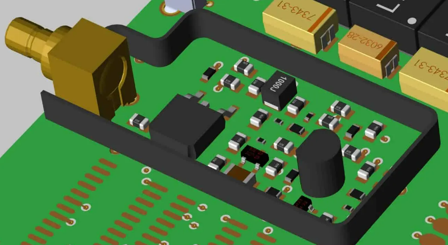
PCB Component Placement Guidelines
Incorporating these recommendations during component placement helps to craft superior PCB layout guidelines that boost signal integrity, circuit performance, thermal relief pad performance, manufacturability, and ultimately, gadget longevity.
- Functional Grouping: Organize the components based upon their function and logical connectivity to help in reducing the length of the trace and optimizing the siganl path.
- Critical Components Placement: Start with putting all the important components on top, such as microcontrollers, memory chips, or power management ICs, to have their routing and signal integrity at its best.
- Orientation and Symmetry: Tilt all parts in one and only way and keep them symmetrical for the sake of simple assembly and good visibility. The alignment of components is also essential to the thermal management of an assembly.
- Signal Integrity: Keep the transmission speed as high as possible and try to keep the signal direction separate to prevent interference and ensure the quality of the signal.
- Decoupling Capacitors: Putting decoupling capacitors as close as possible to the power pins of ICs will result in lower inductance and, hence, improved power distribution.
- Heat Dissipation: Strategically move heat-generating components apart from delicate parts and integrate heat sinks or thermal vias properly in order to facilitate heat dissipation adequately.
- Connector Placement: Generously place the connectors on the edge of the PCB where the cables can be routed easily and where they won’t cause any interference with other components. Sides should be orientation-marked for convenient use.
- Mechanical Considerations: Take into consideration the mechanical components of your prototype, such as enclosure fittings, mounting holes, and clearance for mechanical components or control interfaces.
- Keepout Zones: Specify areas of component positioning that could hamper other operations, such as heatsinks, connectors, or areas requiring access for testing and maintenance, by defining keepout zones.
- Test Points: Have testers use test points that allow message transmission, especially when debugging and maintaining the device.
Layout Design Optimization and Tips
The layout guidelines, assembly drawings and optimization of PCB is critical for performance assurance, production, and reliability. Therefore, implementing these tips and adhering to those best practices will enable you to not only enhance the overall electrical functionality of your PCB but also guarantee that the entire board design is manufacturable and reliable.
- Component Placement: The components need to be fit correctly to have the perfect signal integrity, thermal control and routing. Place the critical part first, which includes signal pathways, power distribution system, and thermal considerations. Place components related to each other close to each other to make cleaner and more durable wiring.
- Signal Integrity: Reduce signal degradation and electromagnetic interference (EMI) by following acceptable vertical and horizontal trace routing methods. Employ short and straight traces for high-speed signals, give corners a wide berth and make sure that trace widths and spacing remain the same throughout. Aircrafts when parking on ground planes and power planes should be well aligned to provide sufficient shielding and reduce noise.
- Thermal Management: Heat up all parts of the PCB evenly to avoid setting a hot spot and keep the components safe. Position high-power elements precisely, consider paths of cooled air, and use thermal vias to cool heat to any inner or outer layers.
- Routing Optimization: Optimize signal tracing geometry to minimize signal distortion, thereby reducing interconnection resistance. Implement these measures, like not allowing traces with different signal frequencies to lie on the same level, keeping trace widths uniform across the board, and reducing the number of vias. Apply differential pairs for fast data signal transmission to enhance its immunity to noise.
- Design for Manufacturability (DFM): Consider manufacturing constraints at the early design stage to prevent expensive rework. Adhere to PCB production standards like the minimum trace width, clearance clearance requirements, and PCB stack-up layer specification. Use DRC and DFT rules design to guarantee manufacturability and testability.
- Grounding and Decoupling: Employ suitable grounding procedures to minimize interference through ground plane loops and EMI. Employ a solid ground plane and cater multiple ground connections for high-current sub-systems. Place capacitors around an integrated circuit’s power pins in order to filter noise and ground the voltage levels.
- Component Orientation: Create aligned patterns of components to ease assembly and inspection stages. Define the same component footprints and markings to be used to enable component identification and placement.
- Documentation and Collaboration: Ensure all aspects of the design are thoroughly documented with careful annotations, component datasheets, and fabrication notes. Collaborate with PCB factories and assembling units to eliminate any unforeseen design constraints and ensure a smoother production line.
SOFTWARE TOOLS FOR PCB LAYOUT
In your cad tools selection, take into account variables like your budget, styling requirements, the user experience you prefer, and the ability to connect components of the tool to work with others. Most of these utilities have a free trial or a community edition, which enables you to check out their possibilities before making the final decision.
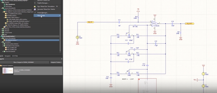
Altium Designer
Altium Designer is multi-functional printed circuit board (PCB) design software that integrates a complete set of features, such as the schematic capture process, PCB layout, PCB routing, and simulation, on a single platform. It includes superior routing tools, 3D visualization and help with collaboration.
Cadence Allegro PCB Designer
Cadence Allegro is a sophisticated package of PCB design applications providing layout, routing and verification structures. It provides the ability to design and route for high-speed design, constraint-driven routing, and signal integrity analysis.
Mentor Graphics PADS
PADS is card layout software from Mentor Graphics which provides capabilities of circuit design, schematic capture, layout and routing. Notably, it is well-known for its user-friendly interface, cost-effectiveness and interoperability with other Mentor Graphics products.
KiCad
KiCAD is an open-source PCB design software suite which comprises schematic capture, PCB layout and 3D visualization features. hackers and small-scale companies like it for its free access and regular updates.
OrCAD PCB Designer
Orcad PCB designer is a part of OrCAD suite of PCB design tools designed by Cadence. It has the ability to lay out, route, and identify components, make circuit boards and simulate schematic designs, with constraints for design-driven engineering and collaboration.
EAGLE (by Autodesk)
EAGLE is a well-known software product for electronic design process automation that comprises schematic capture, arrangement, routing, and simulation subsystems. It is well-known for its easy-to-use interface, large number of components and uniformity of operation with different operating systems.
Proteus PCB Design Suite
Proteus is a PCB software package that includes PCB layout, schematic capture, and simulation functionality. It provides a device for mixed-signal design, 3D visualization, and real-time design rule checks.
DesignSpark PCB
DesignSpark PCB is an integrated program for PCB design basics by RS Components and is further working on automatic circuit board design, layout, trace routing and schematic capture. It is a favorite amongst hobbyists and small businesses alike because it is so easy to operate and inexpensive.
Challenges in PCB Layout Design
The PCB layout design, though quite significant in electronics field, does not come, however, devoid of its share of difficulties. Here are some common ones:
- Component Placement: Configuring the components in a way that’s optimal for both the PCB and signal integrity, thermal relief pattern and manufacturability is a difficult job that needs mastering. The right space scales, along with the multi-functionality of furniture and the constraints of space, become very crucial.
- Signal Integrity: Signal integrity is so significant that the proper operation of the system is guaranteed. Issues could occur where impedance mismatching, signal crosstalking, and reflections happen, as well as in cases of electromagnetic interference (EMI). Proper trace routing techniques positioned to reduce signal losses will have to be employed, accompanied by an analysis of trace lengths and signal paths to minimize vulnerabilities to transport losses.
- Power Distribution: Saving up and planning are equally important as studying. Difficulties begin with trying to decrease the voltage fluctuations, controlling power dissipation in high-temperature localities, and nullifying the noise. Having the correct plane design and capacitor location is the key for carrying out these challenges.
- Thermal Management: Low heat dissipation is detrimental for components’ functional integrity, leading to increased risk of overheating and reduced overall reliability. Problems are associated with the proper engineering of thermal vias, heat sinks, and thermal thimbles; climatic factors also need to be taken into consideration when airflow and enclosures are designed.
- Manufacturability: Design process for manufacturability needs to take into account manufacturing operations like PCB fabrication, version techniques, and component availability. Issues such as achieving DFM criteria, engineering the layout for printing, and identifying parts that are available and easily soldered will be part of the pcb design rules.
- EMC/EMI Compliance: Reliability of the device requires that it be EMC and EMI compliant, which means that it works accurately and will not disturb the neighbors electronic devices. The difficulties are minimizing radiation so EMI is kept to minimum, filtering the impulse, and shielding to give protection.
- High-Speed Design: Developing PCBs for fast signals adds a level of complexity as SIs management, impedance control, and signal skew reduction are included Technologies include, but not limited to controlled impedance routing, differential pair routing, and signal termination, which are essential for communication of high-speed data between computing platforms.
- Design Iterations: During PCB layout process, there are usually more than one iterations to achieve goals and to detect and correct any error that occur during simulation, prototype, or testing. Handling the process of making new designs with deadlines included is a bit difficult, since it can be difficult to do when some alterations require a great deal of new layouts.
- Cost Constraints: Finding the right balance between efficiency and costs has always been one of the most typical PCB issues in this area of design. Component and board design should include element selection steps, layers count and PCB size, considering that the allocated budget does not sacrifice the expected functionality.
- Cross-Disciplinary Collaboration: PCB design reflection with various teams is often engineer-inclusive notably electrical, mechanical, and fabrication experts. Allocating enough time and attention to team communication and coordination is necessary inspite team members’ different expertise, especially for PCB design projects.
Conclusion
To sum up, producing good PCB layout guidelines is a complex process that should never be overlooked, as it can determine the performance and reliability of electronic equipment. This implies that the establishment of such a CAD system involves overcoming barriers including board layout, communication integrity, the ideal source of power supply, thermal issues, and regulatory and manufacturing compliance. Nevertheless, even the efficient PCB layout guidelines face many obstacles. How to take account of the design constraints, use appropriate design tools and cooperate among interdisciplinary teams will lead to this result. Through the right solution to the given challenges, designers can develop PCB design rules that comply with performance parameters, maintain adequate budget and time planning and eliminate reliability and functionality problems in the electronic systems they are meant to support.