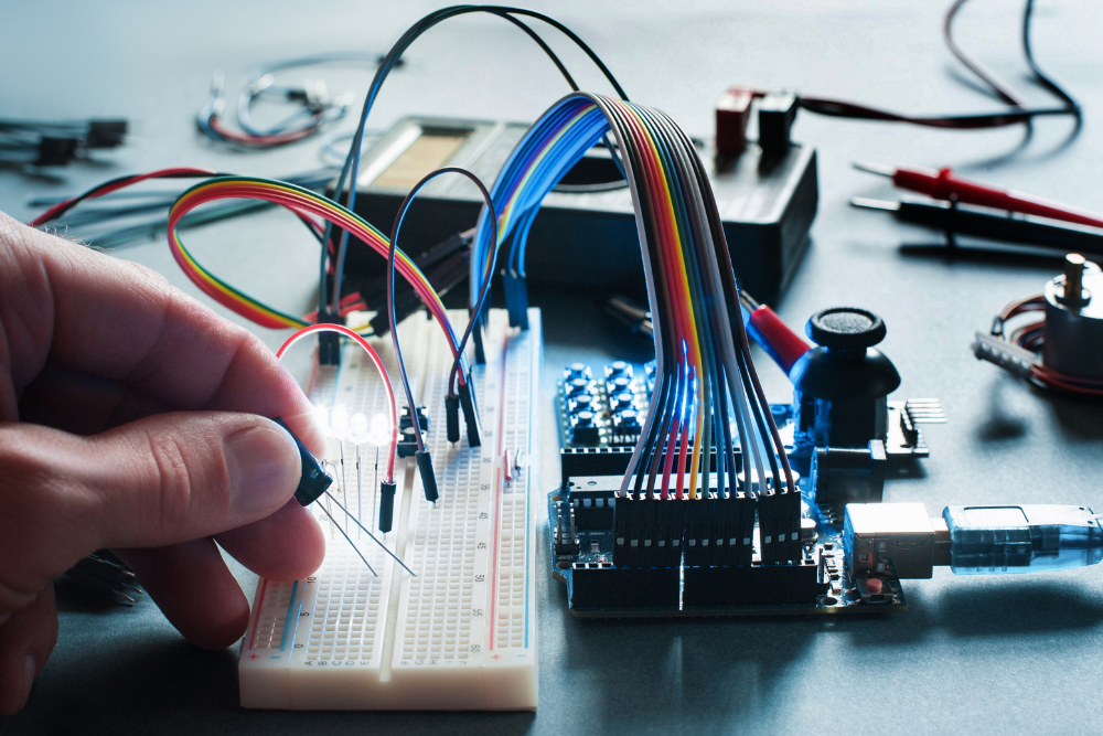
PCB (Printed Circuit Board) design is the most complicated and indispensable stage in the manufacturing of electronic devices, involving keen observation, prediction, and technical know-how. The importance of a carefully planned PCB layout design can’t be overemphasized. It facilitates optimum operation, dependability, and, when necessary, the manufacturability of electronic devices. In this tutorial, the specific PCB layout design tools are discussed, which are at the heart of the electronic circuit engineering discipline and produce more competent and reliable electronic devices.
What is a PCB design layout?
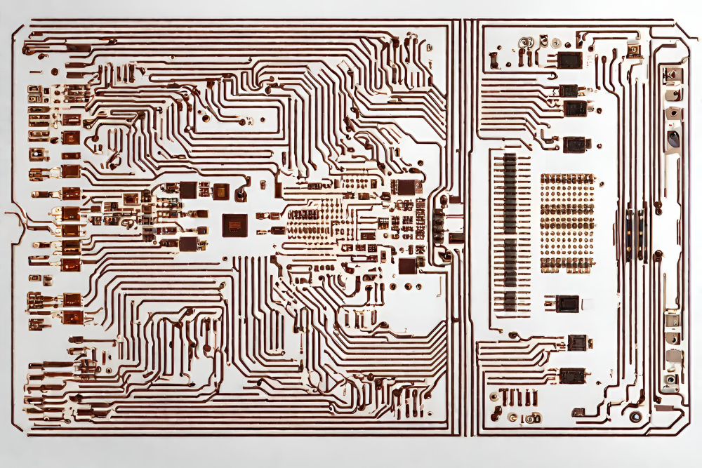
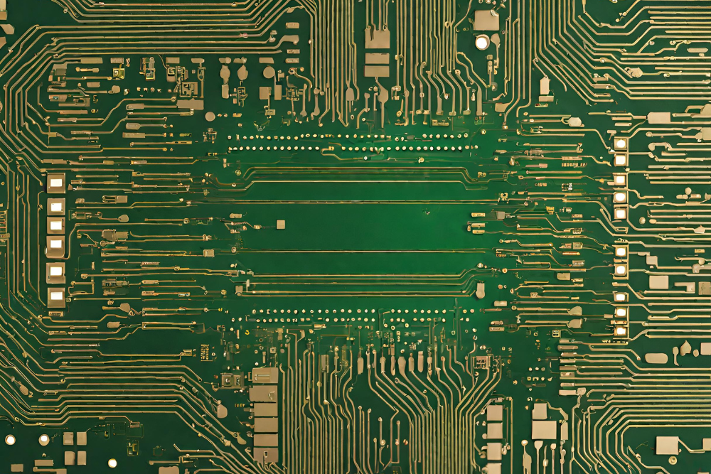
Electronic component and trace spatial layout guidelines on PCBs and other elements in the PCB design layout process are a basic feature of a human being, particularly on a printed circuit board (PCB). Obviously, it is a matter of embedding the components thoughtfully to achieve EMIE signal quality, correct thermal behavior, and optimize manufacturability. However, taking advantage of the component placement stage in the PCB design, the engineers use PCB routing of electrical traces correctly and make functional electrical pathways within the specification. The pathways should not violate the design rules, which will be an indicator of reliability and integrity. Other design dimensions being addressed are power distribution, which involves the use of ground or power planes, decoupling capacity, and regulators to provide a stable and clean source of power to the components. Heat emissions, which are produced by the placement of heat-emitting components and the vias of thermal control, prevent PCB layout designers and developers from heat buildup while also taking into account heat dissipation across the PCB.
Additionally, issues related to PCB manufacturing being taken into account help engineers choose ways that would be suited for quick printing of assembly drawings and integrating circuit board assemblies, whereas detailed documentation contributes to effective collaboration, fault diagnostics, and future problem revision. Overall, a meticulously accomplished PCB layout design serves as the template for the creation of the actual printed circuit boards, taking into account the electrical, thermal, mechanical, and manufacturability properties in one form or another and therefore constructing a functional electronic device.
What are the basic printed circuit board design steps?
The design and manufacture method of a PCB (printed circuit board) comprises many key stages to be certain that we end up with a functional and trustworthy assembly in the end. Here are the basic PCB design steps:
- Requirements Analysis: Start by procuring and studying the specifications concerning PCB manufacturing, which entail the circuit design diagram, the exact component pins and trace width specifications, the electrical design standard, the mechanical constraints, the electronic components, and any other applicable industry standards or laws.
- Schematic Design: Create schematic symbols in a PCB schematic diagram, employing the aid of the schematic data entry software. This consists of illustrating the connections between components by depicting certain elements while others are connected to them by way of electrical nets.
- Component Selection: Select proper active components based on circuit design needs, which include ICs, transistors (or other active parts), resistors, capacitors, and so on, while also adding other necessary parts, such as connectors.
- PCB Footprint Creation: Create or identify footprints for the IC in the schematic as well. Position marks the individual parts of the PCB via a footprint definition that captures both physical size and pin placement.
- PCB Layout Design: Position components on the printed circuit board layout software based on the schematic drawing, among other things, such as the signal integrity, the thermal management, the power distribution, and the manufacturability. Route electrical traces to arrays or relays that will enable the entire system to connect components while following the PCB design rules and guidelines.
- Routing: Interlace connections between components in accordance with the component diagram, and a scheme of electric routes will be set. Observe the recommended practices for aligning the passage of high-speed signals, dealing with interference signals, and utilizing the signal quality control process.
- Design Verification: Do design rule checks (DRC) and electrical rule checks (ERC) to eliminate the possibility that the designed pattern does not meet certain PCB design rules and specifications. Conduct a check to ensure the execution for digital signal strength, circuit performance, power distribution, and manufacturability are in conformity.
- Prototype Fabrication: Generate manufacturing files for fabrication (gerber files, drill files, etc.) using the PCB layout graphics and send them to a PCB fabrication vendor for prototype PCB production. Review and conduct fabricated PCB inspections in order to see that they conform to the specified design.
- Assembly: Create a prototype PCB in stages through wave soldering of PCB circuit board components onto the board as per the assembly instructions. Validate the layout of components and solder mask connections to make sure all of the items are in the right place and there are no inconsistencies.
- Testing and Validation: Make a full assembly test of the PCB to ensure that it functions well, accelerates, and withstands a long period of time. The operation of electrical tests like continuity checks, functional tests, and signal integrity analysis must be carried out so as to confirm that the PCB is satisfactory per its design requirements.
- Iterative Refinement: Conduct test runs if needed, and obtain results and feedback in case there are missed points or failures to fix them. Perform the necessary revisions to the schematic and optimize for the purpose of performance, reliability, and manufacturability. In order to accomplish this, the schematic would have to be altered again as a means of achieving all three.
Foundational Principles of PCB Layout Design
Introduced in the layout design, principles are necessary design rules and practices that thus lead the designer to the end of the successful accomplishment of the printed circuit board (PCB) layout design. These principles, which cover a wide range of PCB layout aspects such as signal integrity and power distribution, thermal management, and manufacturability, as well as reliability, are the pillars of the entire pcb layout design process. Here are some key foundational principles of PCB layout design rules:
1. Component Placement
Strategically placing critical components is very important to route signals, minimize the horizontal trace routing lengths, and provide better thermal control. Group similar items together for ease of understanding and look at the functional relationships of parts forming the communicating chain when making design decisions.
2. Signal Integrity
For signal integrity purposes, minimize the signal reflections, crosstalk, and EMI by providing a suitable grounding and routing on PCB layout. Provide the correct trace routing technique, impedance matching, and power and ground plane design to obtain the integrity of the signal layers and reduce signal degradation.
3. Power Distribution
Develop a reliable power supply management system that will ensure power consumption across all PCB components and minimize power drops. Apply a combination of ground or power planes, decoupling capacitors, and low-impedance paths to have a well-regulated and stable power supply, which sensitive components need.
4. Grounding
A good ground plane plan that serves as a low-impedance in-hand ground and power plane for signals and prevents ground-looping should be used to accomplish this. A continuous ground plane can serve as a return path for signals when bends are needed in the layout. Vias can be incorporated to provide valve trace connectivity between the signal return path and the ground planes.
5. Thermal Management

Develop the printed circuit board (PCB) setup to enable easy heat dissipation and to handle thermal issues. Accomplish that by placing heat-releasing and through-hole components appropriately, transfer heat to the inner layers using thermal relief pads or to the heat sink through the hole components, and maintain good airflow and ventilation so that the components cannot overheat.
6. Routing

Improve the routing of signals to reduce overall trace width, lengths, impedance mismatches, and interference, effectively leading to a more signal-integrity network. Implement the speed signal routing instructions and trace widths as well as clearances; observe signal routing in CPU and HDD areas; use smooth curves instead of sharp angles and right-angle bends.
7. Design for Manufacturability (DFM)
Also, check the parallel processes of manufacturability periodically at each stage of the design process to ensure that there are no fabrication problems. Comply with PCB making constraints, e.g., the lower bound of trace widths and clearances; do not create a convoluted or unsuitable design.
8. Reliability
Develop a PCB layout that is able to stand the test of time and withstand harsh environments. Master the use of good solder mask joints, ensure the bordering edges of components aren’t accidentally hampered, and examine the mechanical stress and temperature cycling effects on component reliability.
9. Documentation

Create and maintain a document that has the whole design of your PCB layout, like schematics, component placement, routing, and layout guidelines for placement and constraints. Well-documented code ensures significant collaboration, solves hurdles, and manages future updates.
10. Testing and validation

Conduct through EFT and validation of the PCB layout to ensure its functionality, performance, and compliance with design requirements. Illustrative tools, model testing, and design reviews can be used at earlier stages of the process to identify and resolve design issues.
How do PCB layout design techniques contribute to the overall performance and reliability of electronic devices?
PCB layout design techniques are one of the most important parts of the process that is responsible for obtaining the adequate performance and reliability of electronic gadgets. By carefully using these techniques, engineers begin to get a tool that can help control and develop the details crucial to electronic system performance and lifetime. As controlled impedance routing and efficient signal path control made signal deceleration and electromagnetic interference less likely, the device’s performance was supported.
Thermal management solutions, including the application of either heat sinks or spontaneous heat sinks, are thus applied. Effective thermal management techniques, such as thermal vias and strategic placement of the components, efficiently dissipate heat, which in turn avoids device failure due to thermal breakdown. It helps improve device reliability. Appropriate power distribution networks and integrated circuits with correct decoupling capacitors and low-impedance power planes maintain equivalent power supply levels without power disturbances, providing a solid base for efficient energy supply.
Optimizing Component Placement on a PCB
It is important that an optimum layout of component placement on printed circuit boards is implemented so that both optimum results, as well as reliability and production, can be realized during this time. Several factors should be considered during this process:
- Electrical Performance: Put components so that overall horizontal trace routing lengths are as short as can be and the transmission line impedance mismatch is minimized, particularly in high-speed or high-frequency circuits. Clustering the related components reduces parasitic capacitance and inductance, which makes the signal path longer.
- Thermal Management: Place heat-generating devices in such a manner that they are easy to heat up and dismantle effectively. Try airflow, thermal vias, thermal relief patterns, and heat sinks for an even distribution of heat, which avoids localized overheating and thus component reliability.
- Signal Integrity: To avoid the risk of EMI between high-frequency signals and power supplies, as well as other noise-producing parts such as high-current traces, switching components, and sensitive component placement towards the signal source. This will maintain signal integrity. Take into account commonly accepted signal routing methods and grounding rules to have little or no amplitude distortion, crosstalk, or impedance discontinuity.
- Mechanical Constraints: Consider mechanical factors such as the enclosure size, the height of the various components, and the assembly procedures that need to be followed. Assemble the components so that they are easily mounted or repaired during assembly and maintenance with no interference from neighboring components or outside structures.
- Manufacturability: Plan the layout of devices so that all their passage to printed circuit board design assembly processes (soldering, inspection, testing) will be smoother. Take this into consideration during production and prevent simple parts from being tucked within complex component orientations or inaccessible locations.
- Component Accessibility: Place components to simplify accessibility for all the operation phases, such as diagnostics as well as repairs and regular supporting maintenance. Take into consideration test points and connectors as well as interfaces for programming when routing through the PCB assembly. Make sure that it can’t be done without the removal of the PCB assembly.
- Thermal Expansion: An example of the parameters considered to avoid the mechanical stress or soldering process of joint failure as a result of temperature fluctuation is the one with a different coefficient of thermal expansion of the components on the PCB board.
- Component Interactions: Decouple the components having different functionalities and remove interference-sensitive components from these neuronal clusters. Electromagnetic compatibility (EMC) requirements constitute the main source of interference and have to be considered to make components and subsystems function properly.
- Routing Space: Provide finite room for wires, power buses, and signal return signals. Position the elements accordingly with the goal of avoiding signal interruption at the connections and wires, ensuring framework signal integrity.
- Cost and Component Availability: Consider both the requirement’s performance and its cost dimensions with part availability for excellent results. The optimum positioning of components will save up on the PCB area and therefore reduce the cost of materials, with a corresponding utilization of reliability and functionality.
What strategies are effective in minimizing electromagnetic interference in printed circuit board (PCB) designs?
Minimizing electromagnetic compatibility (EMI) is the key issue that should be considered in the PCB design process in order to avoid problems with the reliability of electronic devices. Several strategies can effectively reduce EMI and enhance EMC (electromagnetic compatibility) performance:
- Proper Grounding: Place a good plane (especially in inner layers) in the PCB layout guidelines to form a low-impedance way to signal and get rid of guard loops. Apply a ground plane that is continuous, and make sure all the components connect to the ground plane with a stable and low-induction process.
- Signal Integrity: Maintain your signal quality by implementing signal routings with care and eliminating signal reflections wherever possible while impeding signal coupling between traces. This way, impedance matching, controlled impedance routing, and observation of the designated signal paths should be followed.
- Shielding: Counter the radiation of electromagnetic fields from their sources via barrier techniques, thus protecting against radiation and coupling into sensitive areas of a circuit. Shield the systems or subsystem components with sliding metal enclosures or shielding cans to reduce emissions of EMI and the system’s susceptibility.
- Ground Plane Design: One creative idea would be to match the horizontal and vertical traces of the copper layers of the PCB as a ground plane so that low-impedance referencing can become possible. Distribution signal traces over the ground plane for improved high-frequency loop and reduced loop inductance would result in decreased radiation of electromagnetic emissions as well as more signal immunity to external noise.
- Component Placement: Identify the most suitable places on the PCB layout to make sure that noise does not interfere with the potential sources or sensitive signals. Be sure to keep noisy factors such as switching power supplies and pulse-width modulated control signals as far as possible from the design of analog and RF work spaces to suppress intrusion.
- Filtering: Put into practice the passive filtering elements, for example, ferrite beads, capacitors, and inductors, to take away the unwanted noise and harmonics from the power and the signal lines. The proximal area to the noise source or vulnerable components may be chosen to house these components, such that little of the EMI seeps into the overall system.
- Grounding Techniques: Implement star grounding or grounding island techniques to realize a mode of operation where noisy elements are isolated from each other on different circuit blocks. This way, field disturbances are isolated, and the avoidance of loops on the ground can be expected.
- EMC Compliance: Develop PCB layouts that are compliant with EMC guidelines and legislation that are designed for the target application. Do EMC tests and validations to check if the given PCB design advantages meet the emission and immunity needs in a real-world running state.
- Signal Return Paths: Note that the return signal paths must be followed by a direct low impedance to the source. Rather than loop areas, use rectifying paths, and through shortening loops, you will actively decrease loop inductance and minimize radiation and electromagnetic fields.
- Crosstalk Mitigation: Avoid signal line interference with adjacent traces by maintaining correct spacing between data lines, controlling impedance routing, and implementing differential signaling between high-speed data lines. Toggle cross-talk can lead to the appearance of unwanted noise and interference in nearby circuits.
How does PCB layout design impact the manufacturability and cost of electronic products?
The role of board layout design deserves special attention, but it is what is used in determining the cost effectiveness and the manufacturability of electronic products. Here’s how PCB layout design impacts these aspects:
Manufacturability
- Component Placement: The placement of components is an important stage for this particular manufacturability. There should be a board layout with functional capacities such as automatic machine pickers and soldering. To enhance reading comprehension, providing context, rephrasing sentences, utilizing synonyms, and incorporating cross-references or examples will help learners better understand and recall information. Placement of production elements in the wrong manner can lead to assembly mistakes, increased setup time, and higher labor costs as a result.
- Trace Routing: As part of a good fab design process, consistent routing of the signal is needed. Prototypes should conform to the maker specifications to maintain their ability to be constructed electronically without etching that is more than optimal, for instance, or even soldering process problems. By providing regular lines in the design, the risk of a defect during manufacturing is reduced, and regularity in the manufacturing is guaranteed.
- Design for Test (DFT): Implementing board-level testability into the PCB’s design makes troubleshooting and test processes during the manufacturing process a straightforward experience. With these test points, boundary scan circuitry, and diagnostic facilities included, it becomes possible to run the tests, debug the tests, reduce the manufacturing cycle time, and improve the product yield.
- Design Rules: Complying with the PCB design rules and directives stipulated by the manufacturer in terms of PCB design will ensure that the layout of the PCB has attributes that meet the manufacturing processes of the company. DRC (design rule checks) are a design verification tool that will discover manufacturability issues early in the design phase, helping to prevent the delays that will occur from expensive corrections.
Cost
- Material Usage: The design of PCB layout is directly related to material usage, so even the total price of electronic products can be affected by the lower cost of materials. The layout design can occur by fulfilling such requirements as minimizing board size, layer count, and copper usage, which will reflect on lowering material costs. Compact floor plans that are implemented to lower the costs of the materials used could be the desired goals for builders and even for developers.
- Complexity: The obscurity or difficulty of the layout design of a printed circuit board is a significant cost in its manufacturing. More labor hours are spent during the fabrication and assembly of intricate partitions, which have a high density of components in addition to the complexity of routing. This means that, finally, labor costs have increased. Making the design as simple as possible during manufacturing, where it is feasible, helps in minimizing complexity and lowering costs.
- Manufacturing Yield: When PCB designs for the quality of manufacture are used, more manufacturing is done and fewer deficient products are produced that need to be reworked. Higher outputs dispose of waste and defects that cost the production phase of an item, thus minimizing the per-unit price.
- Prototype Iterations: Iterative buildup due to redesign costs or manufacturing problems can take longer to market completion, which is accompanied by high costs. An elaborated PCB design, which can cut down the time for prototype iterations, definitely leads to the minimization of these costs, and as a result, bringing the product to market becomes quicker.
- Component Selection: PCB layout design affects component selection, and this is very crucial since the selection of the components affects the costs. Selecting costly but high-performance parts in BOM will keep the BOM cost lower and will be cheaper due to underspecifying. Not only this, but in addition, tailoring component footprint and package type assures the ordering process convenience and minimizes inventory costs.
What tools and software are commonly used for PCB layout design and analysis?

These circuit boards can be designed by computers using a variety of layout design tools and software platforms. This includes many functionalities and features that are suitable for specific circuit designs, depending on the application. Some of the most popular tools in the industry include:
- Altium Designer: Altium Designer is a multiple PCB design software suite that allows engineers to create circuits, layout the layout, create a 3D model, do simulation analysis, and design rule checking. This software has a user-friendly interface and provides all the features needed to design complex PCBs according to the specifications.
- Cadence Allegro PCB Designer: The Cadence Allegro PCB Design software is a widely known tool used for PCB design, with cutting-edge features that are useful for the implementation of schematic observation, layout, signal integrity analysis, and manufacturing goods documentation. It provides top-down architecture, input of constraints, and cooperation with the mechanical environments to offer the final CAD model.
- Mentor Graphics PADS: PADS is a modular electronic PCB design platform from Mentor Graphics, generating the BOM, electrical schematic, layout, routing, design rule checking, and simulation tools. It is gaining popularity for its low cost, integration, and compatibility with other EDA tools.
- Autodesk Eagle: Eagle is an appreciable PCB design programme that includes an easy-to-use interface, schematic viewer, arranging, and placement. It is best for developing small to medium-scale projects and has a repository of elements and examples that can be accessed directly for design creation.
- KiCad: KiCad is a free and open-source electronic design automation (EDA) software consisting of the components that allow for both schematic capture and designing a PCB layout, along with 3D visualization abilities. It enjoys popularity as it is free to download, has a community support system, and also runs on different platforms. This section will discuss the various characteristics and differentiating features of the Linux operating system.
- OrCAD PCB Designer: OrCAD PCB Designer is a tool for PCB design provided by Cadence Design Systems. This tool includes the generation of the schematics, placement of the components on the board, and simulation of the circuitry. The manufacturability of the board can also be analyzed based on the output of the design. It eliminates the tedious work involved in creating a breadboard layout as it offers integration with OrCAD Capture for a seamless design flow of electronic components’ arrangements.
- Altium Nexus: Altium Nexus is a collaborative PCB design suite that permits teams to join forces for the purpose of multi-discipline-intensive projects. Here, it provides support for revision control, reusing designs, collaborative work, and better project administration, which in turn significantly improves the user’s productivity in a multi-team environment.
- Ansys HFSS: Ansys’s HFSS is a high-frequency electromagnetic simulation tool that is used for evaluating the RF and microwave PCBs employing electromagnetic technology. With its 3D EM energy simulator, the software is tailor-made for the fields of signal integrity, impedance matching, and antenna performance.
- Siemens Xpedition PCB: Xpedition is the PCB design software from Siemens’s Digital Industries Software, which is meant for the purpose of giving advanced options for schematic capture, layout, routing, and analysis. It brings a linkage feature with other Siemens PLM software solutions for embracing design-to-manufacturing (DtM) product development.
What are the current trends and advancements in PCB layout design practices?
In this regard, computerized technologies and some of their developments are not the only ones bringing about cutting-edge trends in circuit layout design practices. This is caused by the prevailing technological onslaught, which is equally supported by industry demands and ever-growing design requirements. Here are some current trends and advancements in PCB layout design:
Miniaturization:
Compact and small electronic devices are continuously becoming popular, and thus, miniaturization in PCB layout design has become a necessary thing. Engineers apply the improvements in component miniaturization, HDI technology, and multi-layer PCBs to achieve the board size reduction while maintaining an equivalent or higher level of operating functions.
High-Speed Design:
The expansion of various electronic technologies, especially those using high-speed data communications and signal processing, has caused a boom related to high-speed PCB layout designs. An engineer will use sophisticated signal integrity analytic techniques, controlled impedance routing, and differential pair routing to maintain the transmission integrity of high-speed digital signals, signal at a high level, and exclude signal degeneration.
Integration of RF and Microwave Circuits:
Increasingly, RF and microwave circuits are found in various electronic devices on a mass scale. This is due to the development and growth of wireless communication technologies, the internet of things, and vehicle electronics. Alongside PCB layout guidelines, the RF designers also attempt impedance matching techniques and RF-specific materials to produce better outcomes in the case of RF and microwave circuits on PCBs.
Flexible and rigid-flex PCBs:
The flexible PCB keeps coming into applications where space constraints, durability, and weight reduction are big problems. PCB design experts consider new materials, established design techniques, and alternative production methods for flex and rigid-flex designs to maintain high-quality performance.
Advanced Materials:
An expansive application of a number of materials that support PCB layout design is being done these days in order to enhance the reliability, thermal relief pattern, and performance of the product. With the introduction of new materials with enhanced thermal conductivity, dielectric properties, and mechanical strength in order to satisfy the needs of high-density and high-frequency processes, engineers are searching for materials that can meet the requirements of next-generation applications.
3D Modeling and Simulation:
3D modeling tools and simulators are essential components of PCB design techniques, being used to simulate PCB designs for different vertical markets. They enable engineers to visualize and analyze PCB designs in a three-dimensional space. Advanced simulation techniques like thermal analysis, electromagnetic simulation, and virtual prototyping are capable of giving designers the chance to enhance PBC layouts toward high performance, reliability, and manufacturability.
Design for Manufacturing (DFM) and Design for Assembly (DFA)
The trend now is towards making the PCB works taking into account aspects of manufacturability and assembly, which leads to more effective and printed circuit board traces. Design for Manufacturing and Assembly is being applied in the early design stages to cut the costs of material, reduce lead times and lead to product of supreme quality.
Collaborative Design Platforms:
Collaborative portals and cloud-based PCB design tools have started to be more widespread, allowing open work across network groups on PCB layout projects concurrently. These are tools which give you options to check versions, coordinate the projects and do teamwork, which makes it more complete and improves performance.
AI and Machine Learning:
Intelligent and machine learning solutions are infiltrating the field of PCB layout modeling to take over routine operations, maximize design parameters, and identify design problems. Adoption of such emerging technologies would be very likely to accelerate design process, yield better design quality, and allow engineers to explore new design possibilities.
Conclusion
Altogether, understanding the vital fundamentals and techniques of conductive Electronic Wiring Design is vitally important for Electrical engineers who happen to be developing good, reliable, and manufacturable electronic items. Through grasping basic practices of placement of the components, signal routing, power distribution, and finally grounding, engineers can perform an optimistic PCB and layout process to come up with the desired specs and standards of every project.
Besides applying complex tools like simulation software, 3D modeling, or integrated design platforms, engineers are able to experience innovation through exploration, which helps them build the best way to solve the issue. Implementing technology for manufacturability (DFM) principles from the outset allows for appropriate fabrication and assembly, resulting in cost savings and shortening time for product development. In the end, the process of using experienced PCB plan design skills wisely is the way to go because it results in laying PCBs that are not only functional but also high-performing, reliable, and manufacturable, making the products thrive in the real world.