Find out about the PCB board materials with their amazing characteristics and different niches they’re applicable for in various industries. See how these materials act to keep the system layer board being as optimized as it can, both in performance and in stamina. Renewable energy especially solar and wind sources can help a nation’s future energy needs. The boom in such technologies has resulted in reduction of environmental degradation.
What is a Printed Circuit Board (PCB)?
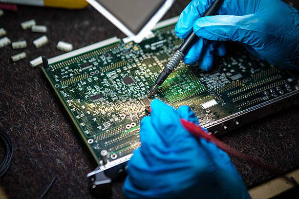
A PCB (printed circuit board) is a flat, rigid circuit board materials made of non-conductive material, usually fiber glass or a composite epoxy material, with conductor traces etched or printed onto its surface. The conductive paths, copper ones, connect the electronic components as divided as resistors, capacitors and integrated circuits. Printed Circuit Boards may be used for mounting and interconnecting of almost every electronic components, and take part in creation of electronic circuits in such kinds of applications as smartphones, computers, GPS systems or in modern automotive and medical equipment.
UNDERSTANDING PCB MATERIALS
PCB materials comprise outer layers, mainly the material of the substrates and the layers produced during the process of PCB construction. Such materials are chosen on basis of various factors like high dielectric constant application, thermal conductivity, mechanical strength, and cost.
Resistors
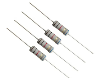
Resistor, which is the passive electronic component that puts restriction on the current flowing into a circuit, is the example of the resistors. They are one of the most important electrical components part of the electrical system used for adjusting the voltage levels and current flow as well as, it acts as a signal attenuation factor.
Capacitors
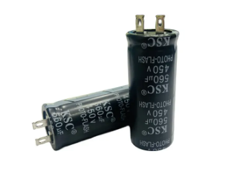
The capacitors are able to store electrical energy and send it wherever they are needed. They block, isolate, keep energy for later use, or even have more functions which perform the operation of signal transfer between different parts of an electrical circuit.
Integrated Circuits (ICs)
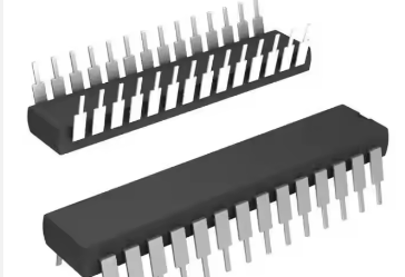
ICs are the highly complex semiconductor components with many electronic functional elements (transistors, resistors, capacitors, etc) placed on the small one-chip circuit. They have multiple tasks to complete, such as amplification, signal processing, logic operations, and storage of logical symbols.
Diodes
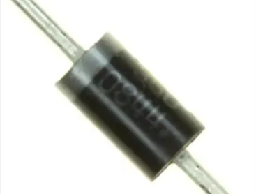
Diodes are a kind of semiconductor component that permits the current to go through it starting from one direction but causes it to be blocked in the opposite direction. Components such as diodes, linear resistors, quadrants, and switches are often employed for rectification, regulation voltage, demodulation of the signal, and switching.
Transistors
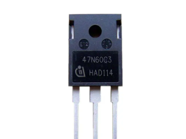
Transistors are semiconductor elements that are employed in the amplification or switching electronic signals. They are able to divert electrons through two terminals, while using a third terminal to control the input voltage.
Inductors
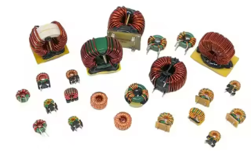
Inductors convert energy involving a magnetic field when the current is flowing and vice-versa. They are functional for filtering, energy accumulation, impedance matching and signal coupling.
Connectors
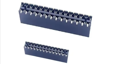
Connectors are used to set up electrical connections between PCB and external components/devices. They have different socks such as the pin headers and sockets and also, the terminal blocks and board-to-board connectors.
LEDs (Light-Emitting Diodes)
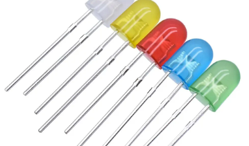
LEDs are semiconductor devices that light will be emitted when current flows through them from forward direction. The function is all purposed for signaling (indication), illumination and visual display in electronics devices.
Switches
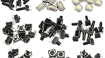
The switches are the electromechanical devices being used as the flow control mechanism in the circuit. Though they may be of simple form, as mechanical switches or complex electric switches, such as BJTs or relays.
Crystal Oscillators
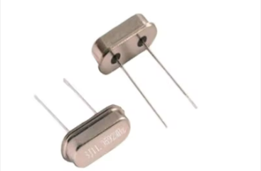
Crystal oscillators generate ultra stable narrow bandishes with very accurate frequency levels. They can be used as time references in electronic circuits like in microprocessor and communication equipment. They can be as the clock signals .
These are just a handful of the numerous components of total flexible and printed circuit board assembly, boards and board assembly part. The choice of the elements is driven by the high degree of customizability required by the targeted devices during this designing phase.
What Materials are used in Multi Layer Printed Circuit Boards?
Multi-layer Printed Circuit Boards(PCBs) are produced by fabricating numerous layers composed of substrate material, dielectric materials, conducting layers, conductive layers, rigid materials, and rigid PCBs. The materials used in multi-layer PCBs typically include:
- Substrate Material (Core):
- FR-4 (Flame Retardant-4): FR-4 is the most common material used for a PCB substrates. It is also a GRP (glass reinforced epoxy laminate) that stands out for his good electrical insulation properties, structural strength, and dimensional stability. FR-4 as the primary structural component in multi-layer PCB, can be also considered a backbone to the circuit.
- Conductive Layers (Copper Foil):
- Copper Foil: Copper sheets, which are only as thick as the electrode layers, are sealed with lamination to create the conductive patterns. Copper is metallurgically chosen due to its high electrical conductivity and across process compatibility with Printed Circuit Board. A combination of multiple layers of copper sheets are utilized in order to establish contact with parts and hence generate complex circuitry.
- Dielectric Materials (Prepreg and Core Laminate):
- Prepreg: Prepreg, is a fiberglass fabric where the epoxy resin is impregnated and applied before the curing process of the epoxy. The ceramic material helps in dielectric layer formation between copper layers in multilayer Printed Circuit Boards. Prepreg material gets sandwiched between stacked-core layers and copper layer foils during the formation via lamination provides electrical insulation and adhesion.
- Core Laminate: The core is made of the same fabric as prepreg, however, the fiberglass reinforcement is missing. It adds the much required additional dielectric insulation and structural support in multi-layer PCBs therefore is a fundamental part of these multilayer Printed Circuit Boards. The subsequent core lamination layers are ensured by introducing copper foils on either side of the layers mentioned above.
- Surface Finish Materials:
- Solder Mask: Solder mask is a protective cover that is covering unpainted copper layer traces and pads to preclude solder bridges and corroding. The sensor is usually made from an epoxy polymer resin resistant to corrosion and it exists in different colors (green/blue/red).
- Surface Finish: Design esthetic materials are provided to clothe the exposed copper wires to keep them from getting rusted and the purpose of soldering is also served by these coatings. Frequently-encountered surface finishes include HASL(Hot Air Solder Leveling), ENIG(Electroless Nickel Immersion Gold), and OSP(Organic Solderability Preservative).
- Filler Materials (Optional):
- Filler Materials: Other multi-layer PCBs might have additives like ceramic or epoxy resin filled into the printed circuit board to give it more mechanical strength, thermal conductivity or to impede fire propagation. The reinforcement textiles of composites are possibly filled with these fibers during the PCB manufacturing processes.
Each of these constituents is carefully chosen by its properties to meet expectations in multi-layer PCBs which use in various electronic domains.
COMMON PCB LAYERS
PCB Layer Technical Terms
Through learning of these technical terms, one will have the required knowledge to both design and manufacture PCBs effectively and to also speak the same language with Printed Circuit Boards manufacturers and designers.
- Top Layer (T): The very top layer of the printed circuit board is the one nearest to the user and is where most of the components are mounted and connected by soldering.
- Bottom Layer (B): The ground layer of a PCB is placed opposite the top layer and is also used for component placement and soldering.
- Inner Layer (N): The internal layers of multi-layer PCBs refer to intermediate layers of the board that are placed between the top and bottom layers. Integrating them into their Printed Circuit Boards provides their boards with conductive paths for routing signals, power planes, and ground planes respectively.
- Signal Layer: Signal layers are circuit board dimensions that support the messages (currents) going between components. The layers are wired and coding electrical conductive circuits, and their purpose is to route signals.
- Power Plane: Power plane of the copper board is a place which ensure the distribution of power among the circuit. The essence is to link up with the polar control rooms of power stations.
- Ground Plane: The ground plane is the part of the PCB, the purpose of which is to provide a stable ground distribution to components and circuits. Such filter minimizes the noise and without the stimulus being distorted in the pathway.
- Core Layer: Core layers are the central parts of the PCB stackup, most often made of fiberglass or composite materials with copper foils bonded to both sides. They act as a support and their layers are signal inner or power.
- Prepreg Layer: The prepreg layers are layers of glass fiber cloth immersed by uncured epoxy resin. They are used to keep a core and another layer together during the board making process which is fashioned at PCB.
- Copper Foil: Copper foil is a thin layer of the copper material that is glued to the substrata. It is normally employed to create tracks or pads on PCB topmost side.
- Solder Mask Layer: Solder mask layers are protective layers which are applied over the copper traces and pads on the PCB to prevent formation of breakages and corrosion.
- Silkscreen Layer: Silkscreen layers are commonly used to print component designators, labels, or any other markings on the PCB surface in order to facilitate its assembly and identification.
- Via: Via is a board-through plating which is utilized for an interconnection between various layers. Among the types of vias, the types can be through-hole vias, blind vias, and buried vias being depending on their connection to the layers.
MOST POPULAR PCB MATERIAL
Preferably the PCB materials are FR-4 (Flame Retardant-4). FR-4, fiberglass-reinforced epoxy and laminate materials, provides high electrical insulation capability, a long-term endurance to mechanical loads, high affordability, and market availability. Unlike many other materials, it offers numerous electronic applications, which is attributed to its reliability, versatility, and affordability.
Why FR-4 is better than other Fiber-Reinforced Materials?
FR-4 is favored over other fiber-reinforced materials for several reasons:
- Widespread Availability: FR-4 is the cheapest and mostly preferred PCB material which is available in the market widely, so PCBs manufacturing became very easy using this material.
- Excellent Electrical Properties: The FR-4 provides a high dielectric strength and a low loss tangent. These features guarantee the high performance level for the electronic devices and the signal transmission over the PCB.
- Mechanical Strength: FR-4 is good in the mechanics properties where it has high tensile strength and always maintains its dimension which are the two of the many more that contribute to the durability and reliability of Printed Circuit Boards made from this material.
- Cost-Effectiveness: Unlike other fiber-reinforced materials, FR-4 is about the premium would make a difference to a wider variety of electronic applications than would the use of any of the others.
- Ease of Fabrication: FR-4 can be machine worked and connected through well-proven PCB manufacturing means, e.g. etching, drilling and soldering. It gives the possibility to produce printed circuit boards needed for product implementation.
In essence, FR-4 incorporates electrical performance, thermal properties, mechanical strength, the afforadability and ease of manufacturing process fabrication, which makes it the preferred choice for PCB production.
Advantages and Disadvantages of Using FR-4 in PCB Manufacturing
ADVANTAGES
- Excellent Electrical Insulation: With FR-4, designers can better isolate conductive traces and components from electrical interference by taking advantage of its excellent dielectric strength and low dissipation factor.
- Mechanical Strength: FR-4 is strong, it has a stiff fiberglass structure and very stable outer characteristics, two factors contributing to the durability and reliability of this material in PCBs.
- Affordability: FR-4 is among the most cost-effective substrate materials (consequently) this makes it a great choice for a variety of electronic applications.
- Widespread Availability: FR-4 is known to be one of the most widely available PCB material and with its wide availability manufacturing FR-4 PCBs should be less costly.
- Compatibility with Standard Processes: FR-4 also can be manufactured conveniently using conventional technology in PCB machines, including etching, drilling and soldering to keep production line running smoothly.
DISADVANTAGES
- Limited Heat Resistance: Though FR-4 can be regarded as a good choice for such applications as high-temperature exposure or in severe environment, this type of PCB may not be efficient in those conditions.
- Brittleness: FR-4 can be more delicate and chocks can be complicated so that when the board is handled or assembled there is additional chance for cracking or fracture.
- Environmental Concerns: The cross-plane lamination of the FR-4 circuits can contain an epoxy resin, which might provide environmental and health issues in case of production and disposal are improperly managed.
- Processing Challenges: FR-4 might need another procedure and processing techniques to reach the superior quality desired in a circuitry performance, mainly in the high speed and high frequency applications.
- Limited Thermal Conductivity: FR-4 displays a rather low thermal expansion performance relative to many other materials that could limit its application in dissipating heat quickly.
Fundamentally, FR-4 is a great material because it is a good conductor of electricity, is strong mechanically, is inexpensive, and is easy to work with. However, it also has weaknesses like low heat resistance, brittleness, and environmental concerns. It is very important to take into account these factors while choosing PCB substrate materials in order to suit certain requirements.
Choosing Hard or soft PCB Substrate Materials
The selection of substrate layer depending on the various factors is the hard and soft PCB substrate materials will rely on the application requirements, environmental conditions, and performance expectations. Here’s a comparison to help you make an informed decision:
Hard PCB Substrate Materials
Advantages
- Rigid Structure: Uses of inert substrates result in rigid PCBs having excellent dimensional stability and structural signal integrity which is required to maintain the shape and form of the printed circuit board.
- High Temperature Resistance: It is possible to heat rigidity substrates higher than soft materials under the same conditions. Thus, rigid PCBs is good for those applications which are exposed to elevated temperature.
- Mechanical Strength: Surface hardness implies chemical strength, bending or flexing-resistance at the same time, providing extended durability and security in stressful conditions.
- Surface Mounting Compatibility: Interconnection layers in the form of a dedicated hard plane surface make it possible for mounting components with SMT and SMD technologies, hence system reliability and ease of testing is driven.
- Better Electrical Performance: Tough substrates usually feature electrical qualities considered improved as opposed to low dielectric constant as well as lower tangent loss which can be beneficial in high-speed and high-frequency applications.
Disadvantages:
- Limited Flexibility: While strong substrates retain their rigidity and do not become pliable and bendable enough to be used for designs wherein a conformal or a Flexible Printed Circuit Board Material (Flexible PCBs) is required.
- Risk of Fracture: The substrates can be brittle and are therefore likely to crack or break under mechanical stresses which makes them vulnerable to reliability issues in some cases.
Soft PCB Substrate Materials
Advantages
- Flexibility: Soft substrates grants room for such designs to have an added advantage of flexibility and conformability to irregular shapes in flexible printed circuit boards which can come in handy where it will fit into tight spaces.
- Shock Absorption: Soft and compliant materials exhibit better shock absorption features thus making them suitable for applications related to mechanical vibration and impact.
- Weight Reduction: Soft materials are usually much easier to carry than more massive and heavy-duty hard ones.
- Cost-Effective: Smooth materials could be less expensive than hard material as it depends on the quality of the PCBs and the thickness of prototyping.
- Enhanced Thermal Management: Soft substrates may better conduct heat in many cases than hard materials such as rigid flex PCBs, so it is possible to enhance heat distributing in some ways.
Disadvantages
- Lower Mechanical Strength: Low mechanical strength of soft substrates largely differentiates them from hard materials and this would have a significant impact on the performance of the modern Printed Circuit Boards.
- Limited Temperature Resistance: The low-temperature resistance of flexible materials is less than the hard materials, where they will not be used in the applications requiring high temperatures.
- Assembly Challenges: The soft substrates offer problems during assembly, more especially with the SMT, due to their flexibility and pliability.
The decision between a hard and soft PCB substrate for your application is eventual and entails a number of factors that include mechanical flexibility copper thickness, temperature tolerance, electrical performance as well as the cost of the material. It’s very much required to carefully scan these parameters and choose the substrate material that suits your requirements the best.
CERAMIC-BASED PCB MATERIALS
The material of ceramic-based printed circuit boards exhibit a vast spectrum of properties that make them appropriate for specific applications that requires high speed, long life and sustainability. Here’s an overview of ceramic-based PCB materials:
- Material Composition: Ceramic-based PCB materials, the majority of which are made from ceramics, like alumina (Al2O3), aluminum nitride (AlN), and silicon carbide (SiC), are examples. These ceramics provide us high thermal conductivity, mechanical strength, and electrical insulating qualities.
- Thermal Conductivity: Ceramics are shown to be several times more conductive to heat than conventional FR-4 materials. This property helps ceramic-based Printed Circuit Boards to effectively conduct heat produced by the electronic devices where run high-power and high-temperature applications, thus, this makes them usable for such applications.
- High-Temperature Operation: Ceramic-based PCB materials can stand much higher temperatures than the organic substrate do. Therefore, it is totally good for the use in the environment with high temperatures such as the automation, aerospace and power electronics.
- Mechanical Strength: Ceramics have shown high mechanical properties such as strength and stiffness and are advantageous in applications requiring a high degree of structural strength and resistance to mechanical stress. It is this special property of ceramic material that makes ceramic-based Circuit Boards more sturdy and long-lasting, especially in very poor working conditions.
- Electrical Insulation: Ceramics have extremely good electrical insulation and make sure that conductive pathways or electronic components are separated correctly on the PCB. This feature is imperative as it prevents short-circuiting and preserve the whole integrity of electronics parts.
- Dimensional Stability: The ceramic materials have small thermal expansion coefficients (CTE) and they are not likely to experience significant dimension changes by temperature variations. The thermal conductivity of these materials is critical because it helps resist expansion or contraction to ensure tight tolerances and accurate alignment.
- Chemical Resistance: Ceramic based PCBs are known to be resistent to chemicals, moisture, and erosion degrading environmental factors, thus making them suitable for those applications that are exposed to corrosive and hard environments.
- Surface Finish Compatibility: The ceramic- based PCB material ranges of chemistry used in the fabrication process also, provide other surface finish options that include gold plating, silver plating, and OSP (Organic Solderability Preservative), proving reliable soldering and assembly processes.
- Cost Considerations: The ceramic- based PCB materials are known to say superior performance and reliability. However, they are also more costly than the other organic substrates comes FR-4. The majority of the expenses arise from the production methods which are used for the manufacture of ceramic substrates.
Ceramics-based PCB materials as a whole are particularly good options for applications that involve extreme heating conditions as well as having a strong mechanical resistance and high reliability. Nevertheless, that brings up their higher cost and their being already adjusted to the production of high value niche industries, where their unique features are of paramount importance.
Conclusion
As a conclusion, the PCB material selection step should not be overlooked in the design of consumer electronics part. It has far-reaching impact, on factors like performance, reliability, and manufacturability of a design.
Classical materials such as FR-4 are somewhat between electrical insulation, mechanical strength and cost efficiency that makes them fit in different applications. Nevertheless, some applications needing higher temperatures, greater frequencies, or extreme environments could better be addressed through non-stainless steel materials such as ceramic-based plates that possess increased thermal conductivity, mechanical strength and chemical resistance compared to stainless steel.
Picking the proper PCB material entails assessment of different application needs incorporating electrical performance, mechanical necessities, thermal management, and budgetary requirements. Knowing the strengths and weaknesses of different materials enables designers to make more educated choices which in rob end increase the system’s efficiency and dependability.