One-stop PCBA Manufacturer in China
20+ Years PCB Assembly Experience, Quick-turn services for prototype PCB assembly competitive price for mass production
- SMT, Through Hole and Mixed Assembly
- Passive Down to 01005 Sizes
- Ball Grid Array (BGA)
- Ultra-Fine Ball Grid Array (uBGA)
- Quad Flat Pack No-Lead (QFN)
- Quad Flat Package (QFP)
- Plastic Leaded Chip Carrier (PLCC) 6. SOIC, Package-On-Package (PoP)
- Small Chip Packages (Pitch of 0.2 mm)
ASSEMBLY TYPES
- Surface Mount (SMT)
- Thru-hole
- Mixed Technology (SMT/Thru-hole)
- Single or Double Sided Placement
COMPONENT TYPES
- Passive Down to 01005 Sizes
- Ball Grid Array (BGA)
- Quad Flat Package No-Lead (QFN)
- Quad Flat Package (QFP)
- Small Chip Package (Pitch of 0.2 mm)
TURN TIMES
- Quick turn (1-5 days)
- Standard (10 days)
- Scheduled Deliveries
QUANTITY
- No Minimun Order Quantity
- First Articles
- Prototype – Production
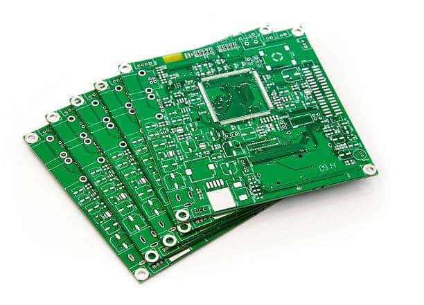
Product Portfolio & PCB Assembly Services
IPC610-D
Standards
ISO9001
Quality products
Over 99.8%
Satisfaction rate
Under 0.2%
Complaint Rate
1-30 layers PCB Fab
PCBA lead time 3-5 day
SMT provides stencil
Electronic Components At least 98% shipping on-time!
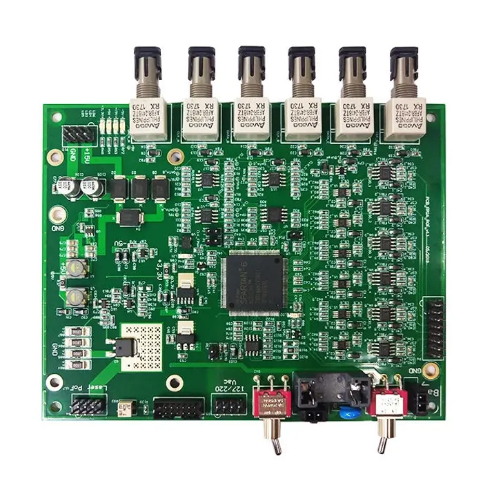
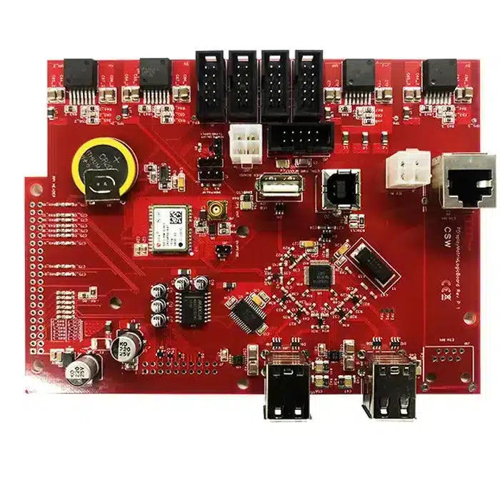
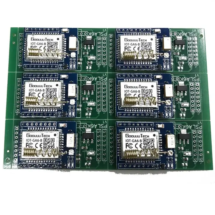
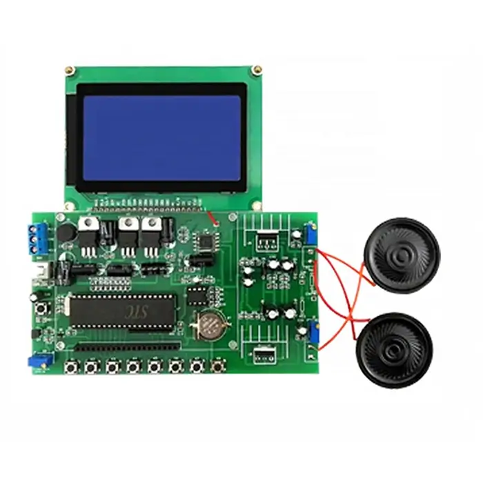
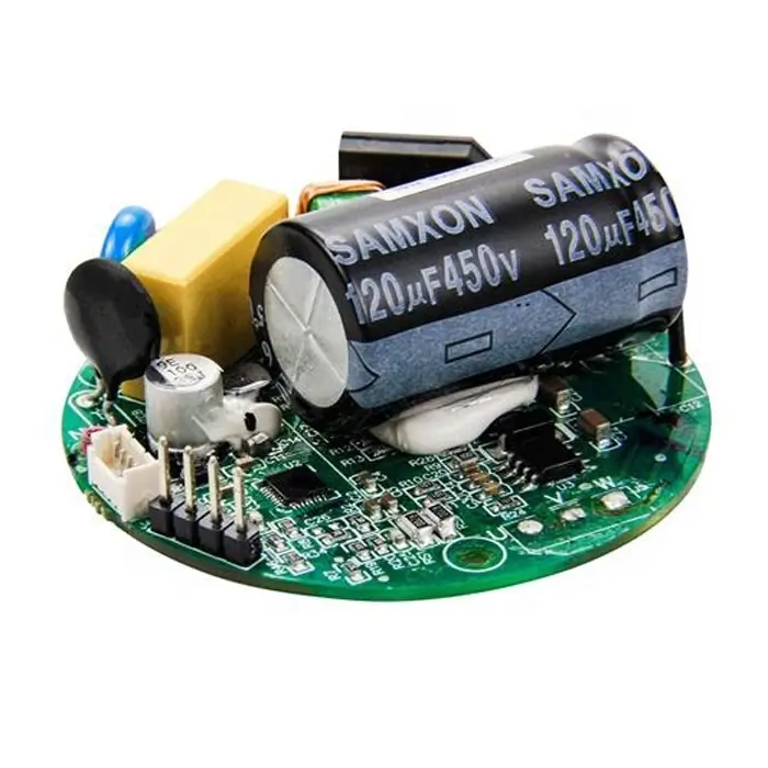
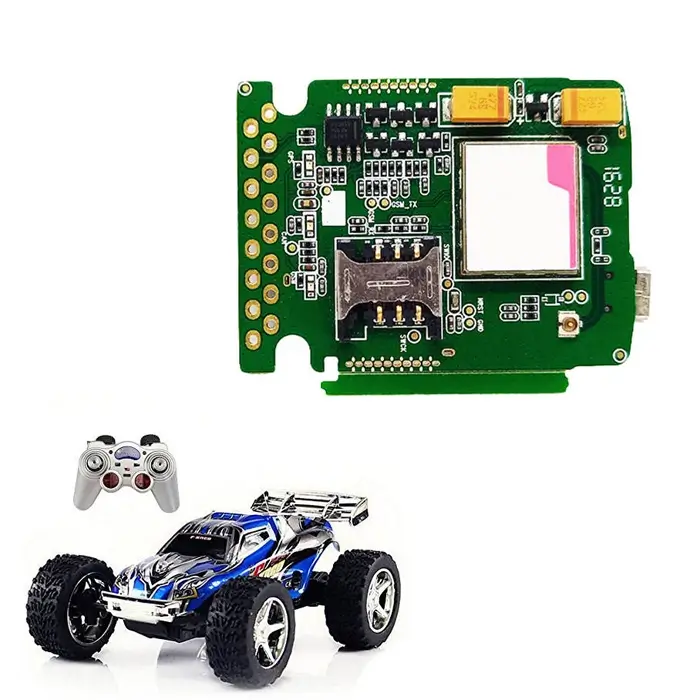
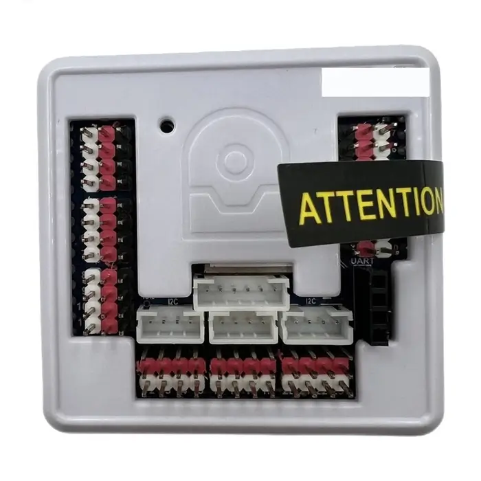
Cable,Box Build Assembly
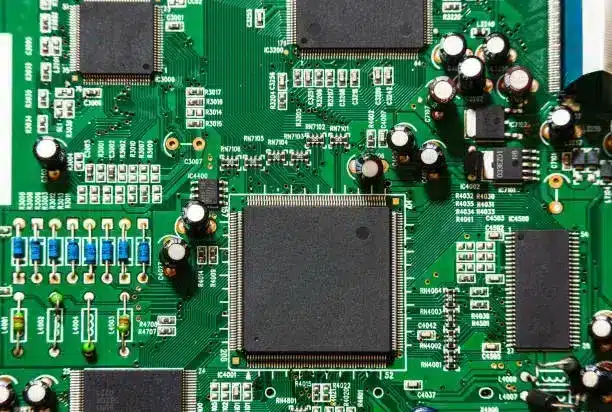
Digital Processor PCB Assembly
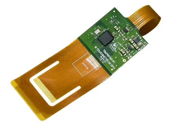
Flex PCB Assembly
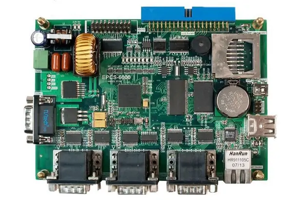
Smart TV Box Pro Board PCB Assembly
Protect your designs with onsite PCB assembly, streamlining the process for prototypes and small-batch PCB assembly.
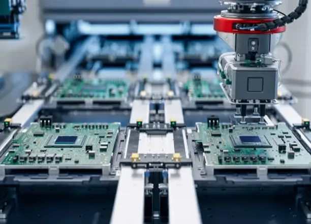
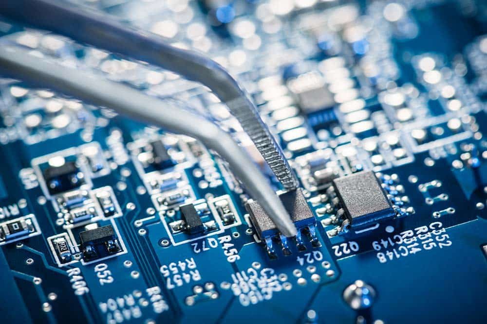
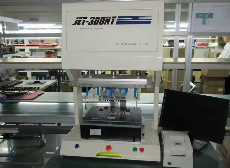
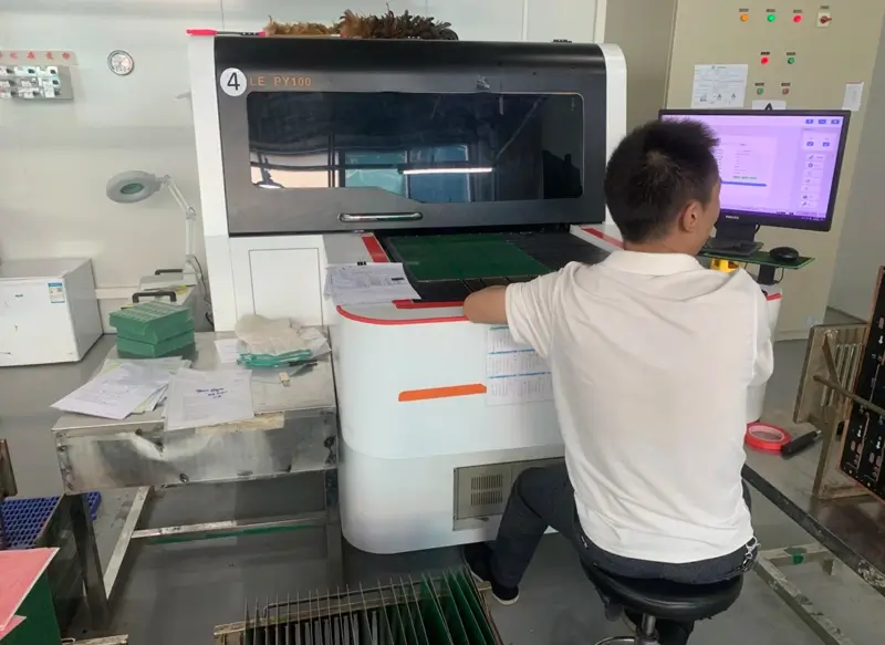
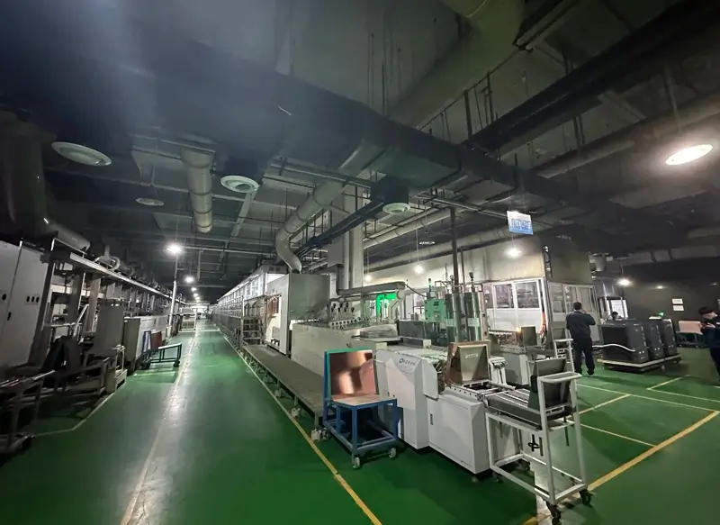
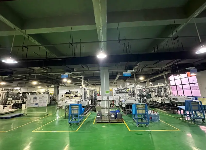
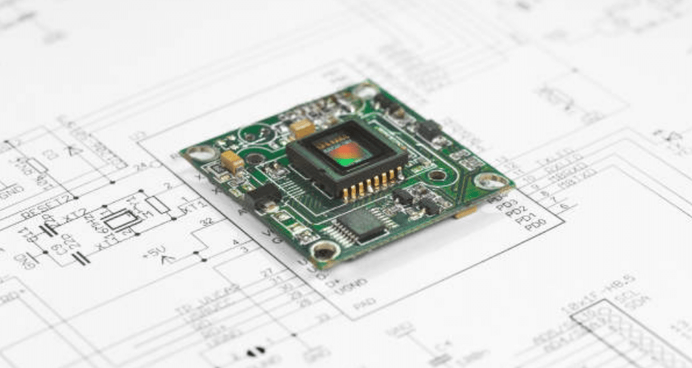
Just like our PCB business, our PCBA services also focus on prototyping and mass production thus making Camtech PCB a one-stop destination for circuit board manufacturing and assembly. This arrangement makes your R&D work easier and more time-efficient. Customer service personnel will link you to professional engineers and technicians who will ensure the best quality as well as the fastest delivery times. We complete customized PCBA orders from around the world every day, with consistently high quality and excellent service, making us an industry leader in PCB and PCBA services. Our factory has developed a lean production management system that combines MES, ERP, IOT, ESD and APIS independently. Japanese imported Fuji placement machines are among high-end devices that we have invested on; others include 3D X-RAY, 3D SPI, our own MES developed in-house IQC incoming material inspection instruments together with intelligent first-article inspection instruments. High-quality PCB ASSEMBLY production services is what we provide.
Camtech PCB Assembly capabilities: SMT Assembly, BGA Assembly, Through-Hole Assembly, Mixed Assembly, Rigid Flex PCB Assembly Services, Electro Mechanical Assembly, Box Build Assembly, Product Assembly, Cable Assemblies. Compliant with a wide range of standards including IPC 610 Class 2 and Class 3.
CAMTECH PCB Assembly Services
Tested. Trusted. Guaranteed.
CAMTECH’s PCB assembly services support all circuit board design complexities from prototype to production volumes. We provide solutions that align precisely with our client’s diverse needs in PCB assembly.
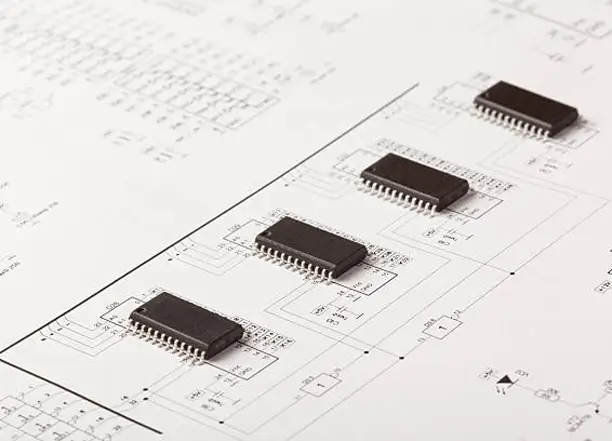
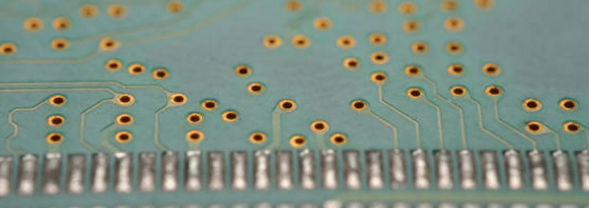
What is a Printed Circuit Board (PCB) Assembly?
A printed circuit board assembly (PCBA) describes the finished board after all the components have been soldered and installed on a printed circuit board (PCB). The conductive pathways engraved in the laminated copper sheets of PCBs are used within a non-conductive substrate in order to form the assembly. Attaching the electronic components to the PCBs is the concluding action to create a fully operational electronic device.
CAMTECH PCBA CAPABILITIES
We deliver complete PCB Assembly services with advanced manufacturing capabilities to fulfill all of your assembly requirements. From prototype assembly to production quantities, bring us your design and walk away with your assembled boards.
If you’re at the prototype stage or are ready for the production build of your circuit assemblies you can trust us to fully support your requirements. When you receive your PCB assemblies from us you can be sure that they have been assembled to your requirements, using the utmost care and attention.
PCB Types For Assembly
- High TG PCB
- HDI PCB
- Flexible PCB
- Aluminum PCB
- High-Frequency PCB
- Metal Core PCB
- Rigid-Flex PCB
- Heavy Copper PCB
Parts Sourcing
- Customer offers all parts (No handing fee)
- Turn-key: All parts sourced by Camtech PCB
- Combo: Partial parts offered by Customer and Camtech PCB sourcing the rest
Assembly Options
- SMT assembly: BGA, QFN, QFP, SOIC, PLCC, PoP, 0805, 0603, 0402, 0201
- Through hole assembly
- Single&Double sides assembly
- Sub-assembly
Soldering Types
- Lead free/ROHS soldering compliant
- Hand soldering
- Reflow soldering
- Wave soldering
Quality Control
- IPC-A-610F class 2 standards
- ISO9001:2015
- IATF16949:2016
- ISO14000
- Free Visual inspection
- X-ray Inspection
- SPI&AOI&ICT(In-Circuit Test) Testing
- Functional test
Order Processing Ability
- Minimum Order: 1pcs
- General lead time: 3 weeks (Exact lead time will be given by the project manager)
- Within 24 hours response after receiving RFQ
- Dedicated project manager for every customer
Turn-key Solution Sourcing
- Digikey/Mouser/TME/Element 14
- Local electronic market
Value-added services
- Designing service
- Mechanical service
- Sub assembly/kitting service
- Drop shipping service
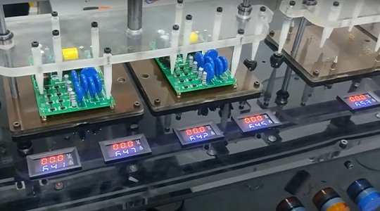
PCB ASSEMBLY PROCESS
CAMTECH PCB delivers complete PCB Assembly services with advanced manufacturing capabilities to fulfill all of your assembly requirements. From prototype assembly to production quantities, bring us your design and walk away with your assembled boards.

1. Parts Procurement / Kitting
The initial step in processing a customer order is to check all the information and data that we receive from our customers. The accuracy and correctness of the Bill of Material (BOM) are critically important since it is used for purchasing the parts.
2. Solder Paste Printing
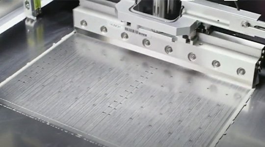
Solder paste is applied to the PCB component pads, using a stainless-steel stencil. In this step, precision is key, as the solder paste must be applied in the correct places using correct thickness to ensure full functionality of the joints.
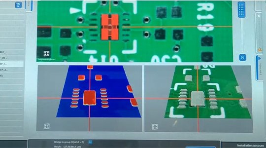
3. 3D Solder Paste Inspection
Due to the complexity of PCB designs containing small components in densely-packed spaces, the inspection stage is a crucial step to ensuring an accurate printing process. Each board is scanned to produce a 3D image, which is reviewed for correct solder paste volume per pad, stains, proper alignment, and the absence of foreign materials that may have adhered to the paste, among others.
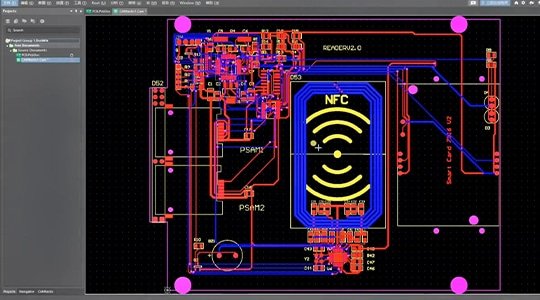
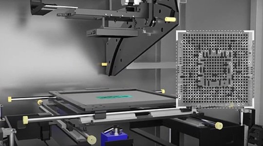
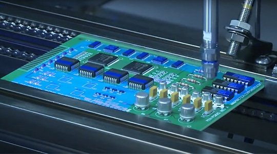
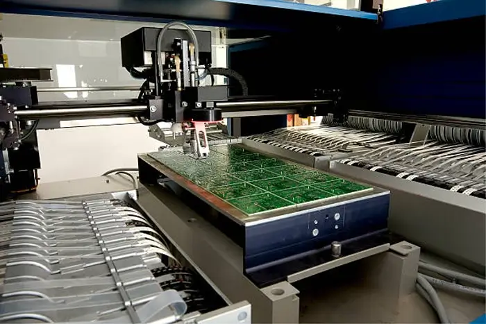
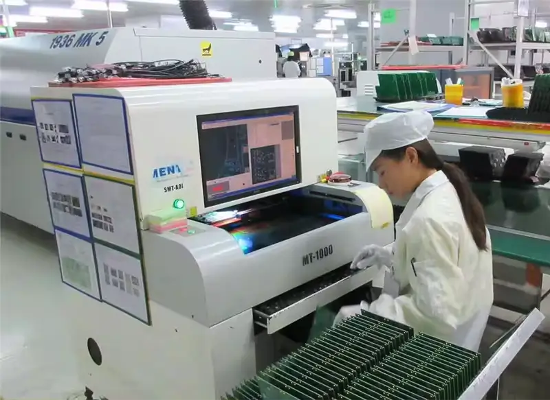
4. SMT Programming
The Surface Mount Technology (SMT) machines are programmed with component placement information. Most often, the program is generated using Centroid files, Gerber files, and BOM data.
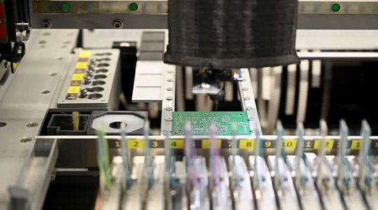
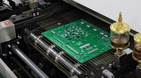
5. SMD Placement
As the PCBs pass through the SMT machine, components are placed onto the pads to which solder paste has been applied.
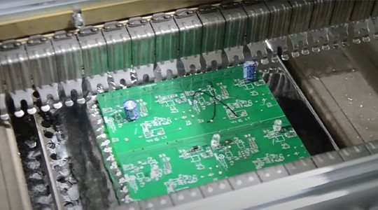
6. Reflow Soldering
At this stage, the PCB enters the reflow soldering machine, where it is held under an infra-red heater in order to melt the solder paste. Once the solder paste solidifies, the components adhere to the contact pads, therefore connecting the joints.
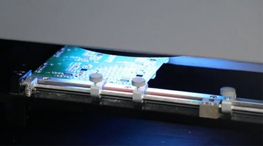
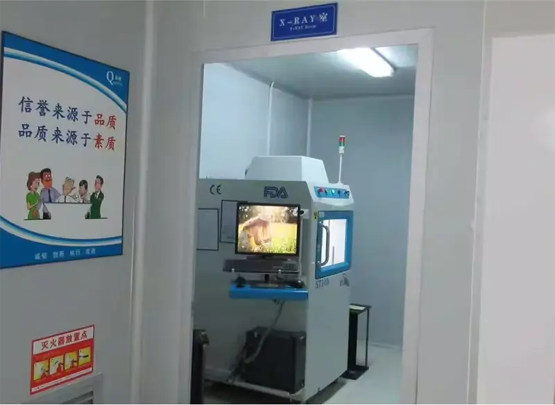
7. X-Ray Inspection
After completing the reflow stage, the boards are sent for X-ray inspection, which is an especially useful method for reviewing complex or layered PCBs. The image produced by the X-ray can be analyzed by image processing software to find defects in the joints – including incorrect amounts of solder paste or skewed component placement.
8. Automated Optical Inspection (AOI)
An AOI machine consists of a series of cameras placed at different angles, capturing the placement of the solder connections. Using image processing software, solders of subpar quality are detected based on how light is reflected off of each solder connection.
9. Wave Soldering
In this stage, the boards are placed on a conveyor belt and passed over a tank of molten solder, which is pumped to create “waves.” As the boards pass over the upwelling solder, the components with leads on the bottom side of the board, which come in to contact with the solder get soldered to the PCB at the same time.
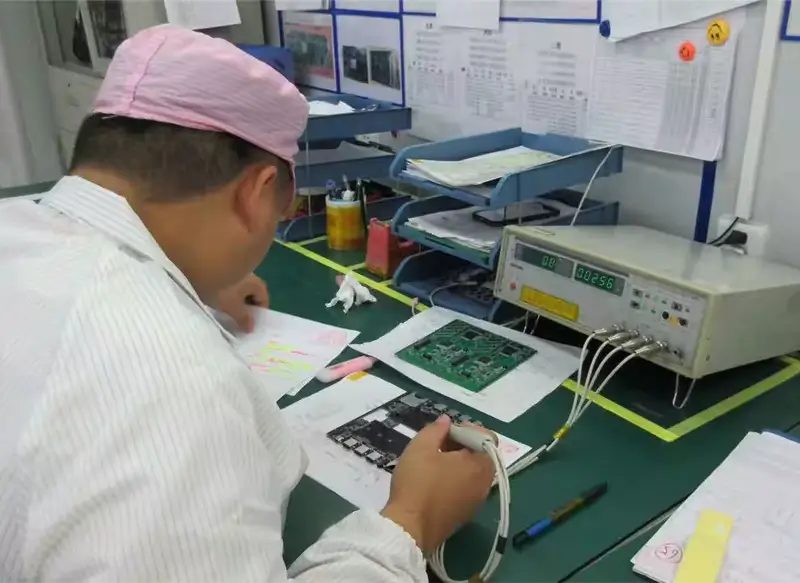
10. Functional Test
After all assembly stages have been completed, the PCB as a whole may be tested for overall functionality. The test is conducted through an interface connected to the PCB that simulates the electrical environment in which the board (as an end product) will ultimately be placed.
11. Conformal Coating
The boards are either dipped or sprayed in conformal coating which is a protective layer that guards against deterioration caused by atmospheric moisture, condensation, contamination, and other occurrences that can damage the PCB over time. This step is important for ensuring the longevity of the boards and the productivity of our clients by preventing corrosion, dendric growth, erosion, and short circuits.
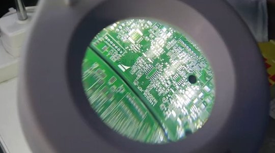
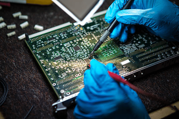
12. Final QC
The final step of the manufacturing process is a 100% visual inspection done under a magnifier. Primarily, the board is checked for soldering and joint defects, cleanliness, flux residue.
One-Stop Full Turnkey PCB Assembly

Procurement
- Stable Purchasing Strategy;
- Authorized Dealers;
- Short Procurement Cycle;
- Full Traceability and Scrap Management;
- Cost-effective Solution.
Fabrication
- 1-30L Bare Board Manufacturing;
- FR-4, Polyimide, Aluminum, Ceramic, Rogers, Arlon, etc;
- 4 layers -10 layers (FR4+Ro4350, FR4+Aluminium, FR4+ FPC).
Assembly
- 52 million placements per month;
- Acceptable maximum board size 680×500 mm, minimum 0.25″x0.25″
- Realizable chip packaging technology DIP, SOP, QFP, PGA, BGA, CSP;
- Speed: 0.15 sec/chip, 0.7 sec/QFP.
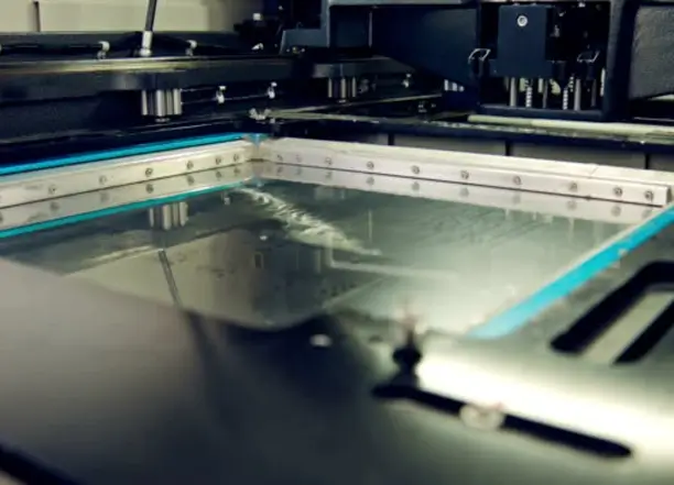
Prototype
- 3D printing completes PCBA prototyping within 48 hours;
- Free Conformal Coating Service;
- Comprehensive functional testing service;
- Accept supplied components in cut-tape or in tray.
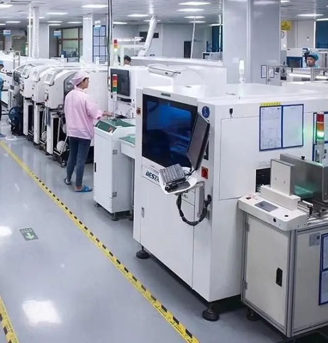
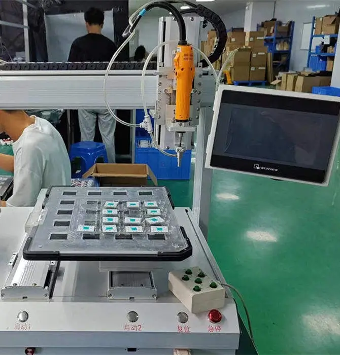
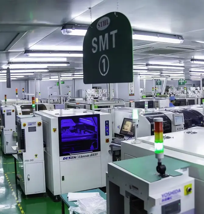
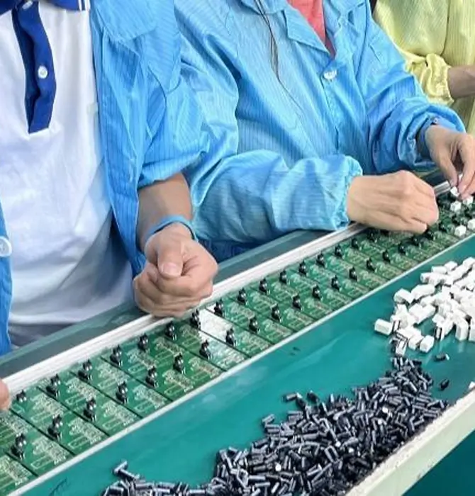
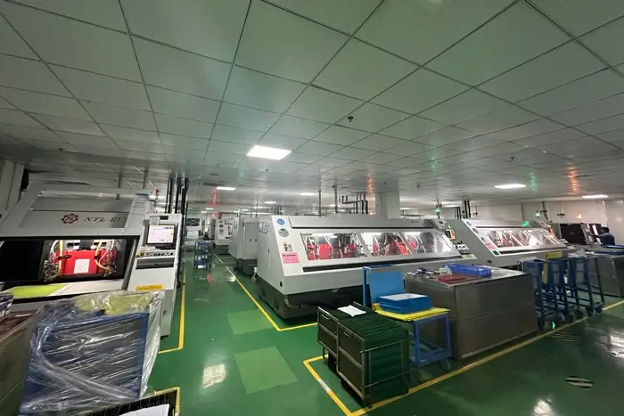
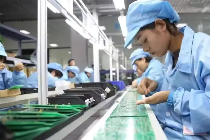
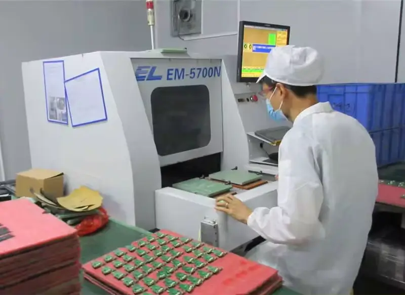
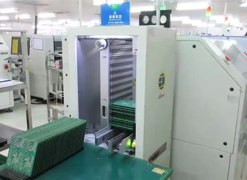
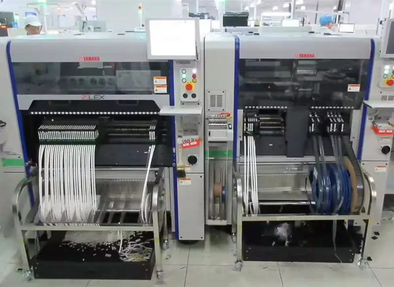
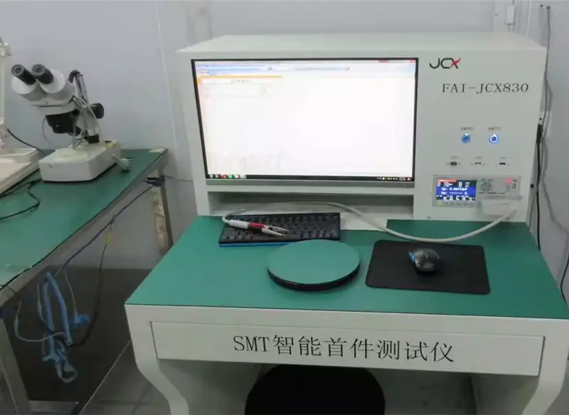
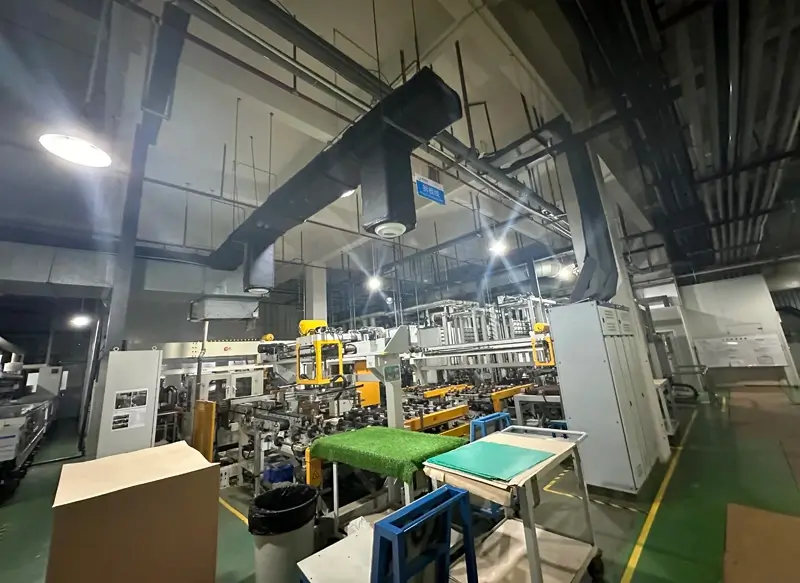
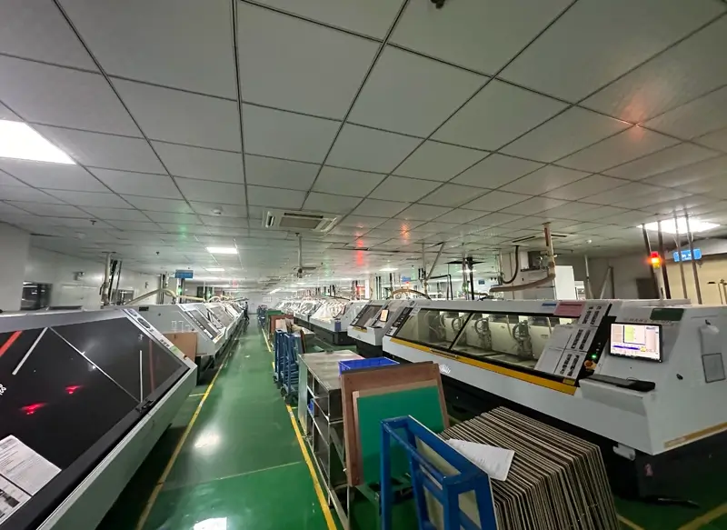
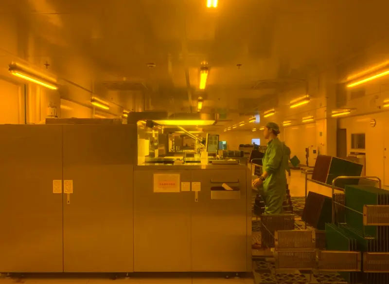
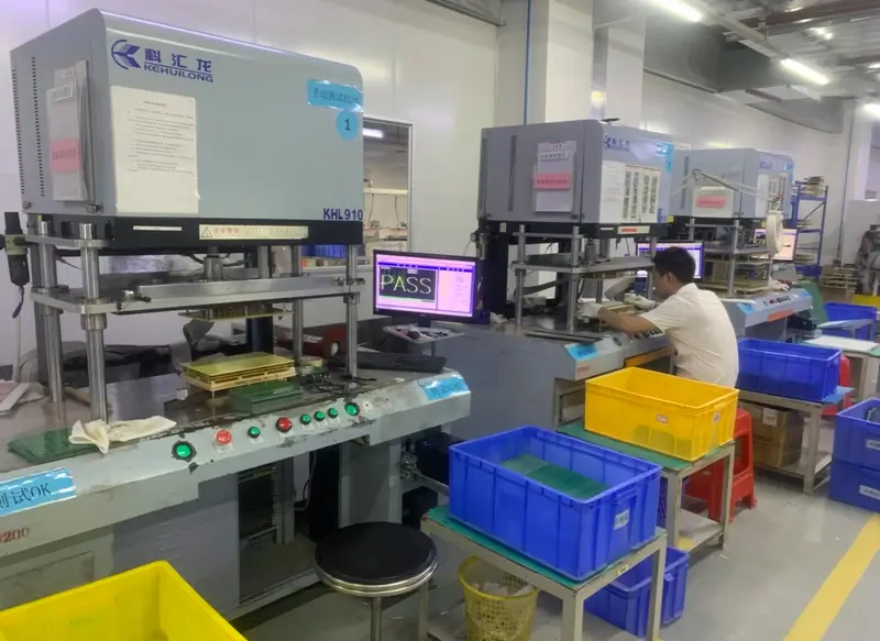
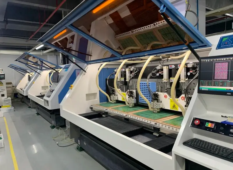
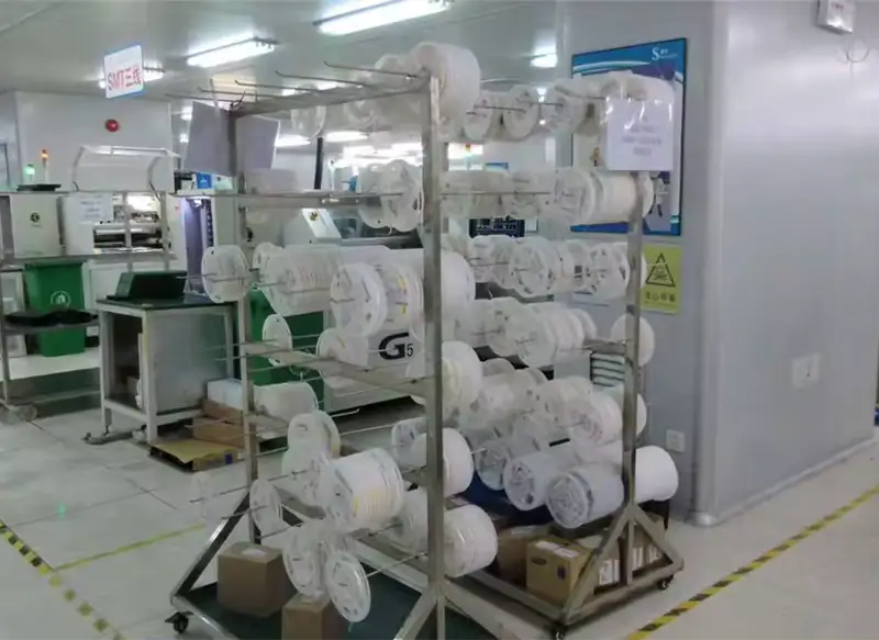
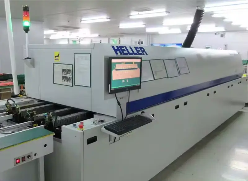
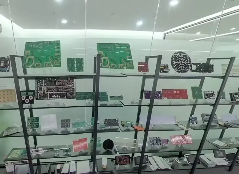
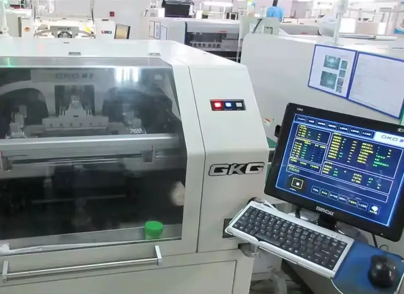
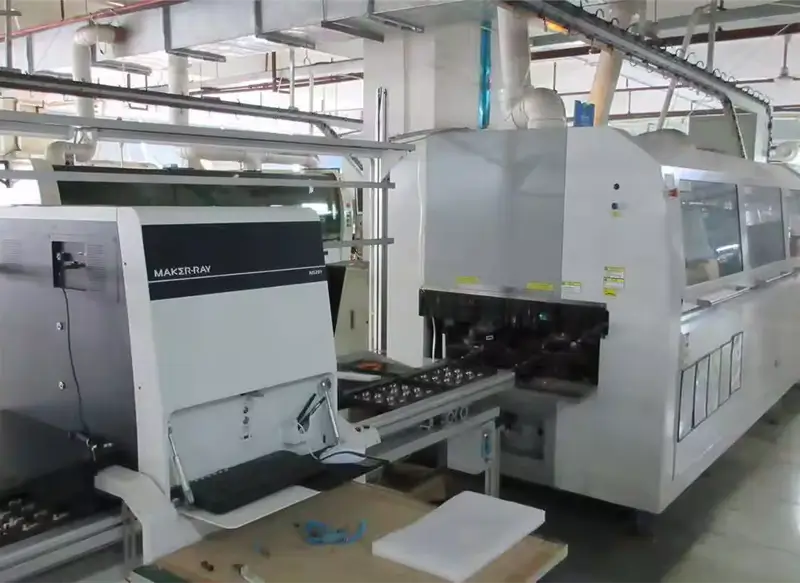
Inside Innovation: Our State-of-the-Art PCB Assembly Hub
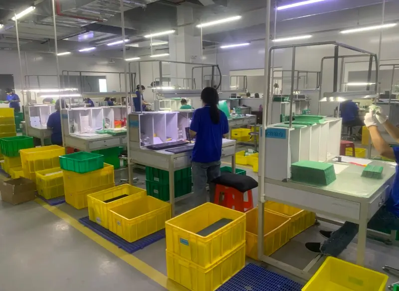
Trustworthy PCBA Manufacturner
Annually serves 300 clients with purchase amounts reaching 50 million USD.
Completed 4,000 one-stop PCBA contracts overseas.
Shared the same PCBA component supplier as Fortune 500 companies.
Latest From The Blog
Step-by-Step: Integrating Via-in-Pad Structures into Your PCB Assembly Process
Implementing Via-in-Pad structures into your PCB assembly requires a step-by-step process that guarantees signals’ dependability and circuit performance. It begins
The Ultimate Guide to Optimizing Your PCB Layout for Efficiency
Printed Circuit Boards (PCBs) are fundamental components in various electronic devices, constructed using different materials to optimize performance and durability.
PCB Board Material Breakdown: Understanding Properties and Applications
The document “PCB Board Material Breakdown: The writing titled “Understanding Properties and Applications” gives information concerning the materials used in