Venture into the accessible realm of circular diameter of the pad for PCB boards via our clear tutorial. From grasping its significance in PCB design to the practical application of techniques that will improve performance, here is all you would ever want to know about these elements. If you are just starting out in design or are an expert, this guide is a sure source of useful tips to improve your skill base.
What is an annular ring?
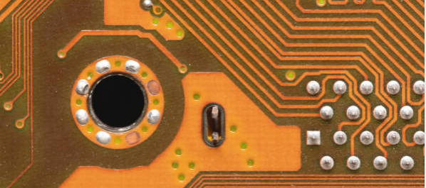
An annular ring is one key element in the manufacture of printed circuit boards (PCBs), which delineates the copper area adjacent to a drilled hole. The copper ring in diameter of the plated holes then acts as the conductor for the circuit traces, making it easy to solder the components to the board. The thickness of the annular ring is another key parameter in the PCB design process; this influences the integrity and strength of the broken trace connection. With a significant annular ring, there is more area available for soldering, which makes the joint stronger and less likely to get defects like solder bridges or substandard joints. Designers exactly choose the minimum ring size, thus considering the production processes, component requirements, and so on, and therefore ensuring the structural integrity and functionality of PCB boards.
Construction of Annular Ring
In the first stage of annular ring construction on a printed circuit board (PCB), holes are drilled through the substrate material, usually fiberglass-reinforced epoxy laminate. At this point, the copper layers are deposited on both sides of the board. When the holes are complete, we remove the rest of the copper that stands around the hole. What’s left is a round copper pad breakout that is located around the hole. This copper plate then presents an annular-shaped ring, which is considered a vital electrical connection point for the part and the circuit traces. The annular ring width is designed to be precise to ensure proper soldering and electrical conductivity during the overall assembly process. Unlike any other component, the annular ring is the most crucial element in the design of the printed circuit board during the PCB manufacturing process.
Types of Annular Rings
There are several types of annular rings commonly used in printed circuit board (PCB) design, each serving specific purposes and offering unique advantages:
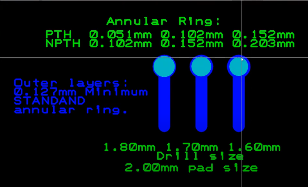
Non-Plated Through Hole (NPTH) Annular Ring: This type of plating is achieved through removing copper around unelectroplated holes and thus creating an annular ring. That is not the point since the pads do not have the copper foil, so the copper is only present in the surface layers of the circuit board.

Plated Through Hole (PTH) Annular Ring: PCB through holes plated thoroughly generate PTH annular rings that surround. In the hole, a copper plating is there, which extends to either side, forming a conductive path between layers.
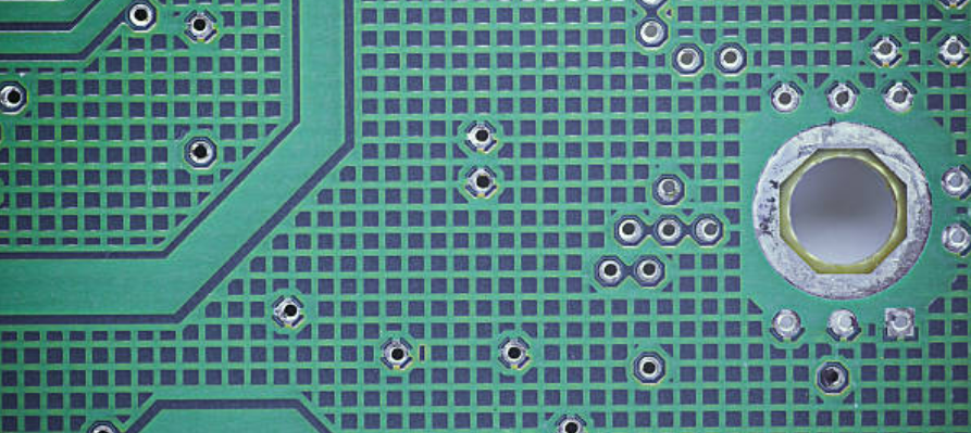
Teardrop Annular Ring: Teardrop annular rings are built to maximize the mechanical strength and consistency of the joint placed between the traces and the pads. This variation features an extended shape, with the trace getting wider as it connects directly to the pad, often resembling a drop of tear. The advantage of this assembly is that it prevents stress concentration and improves the adhesion between the trace and the pad.

Dogbone Annular Ring: Dogbone annular rings that are commonly used in fine-pitch SMT components are mostly suited for this purpose. These involve the addition of the pad for outside the opening, looking like a dog bone. This structure offers improved solder joint reliability and electrical connectivity in a more confined space reserved for high-density PCB manufacturer.

Tented Via Annular Ring: In this case, the annular ring is encapsulated by a solder mask, resulting in the cover or “tenting” of the via. The tents not only prevent solder bridges from occurring but also keeps the overall quality and the most efficient PCB manufacturing process.
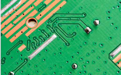
Each type of annular size ring has its own pros and cons, and selection is made based upon factors of application, manufacturing requirements, and design considerations.
Copper Pad on Annular Rings

A copper pad on an annular ring is a vital component of a printed circuit board (PCB), encompassing a circular copper area surrounding a drilled hole. Essential for through-hole components, these pads provide a larger surface area for soldering component leads to the PCB, thus enhancing both mechanical strength and electrical connectivity. Critical in high-density PCB designs and environments with elevated mechanical stress, the size of the annular ring, along with the copper trace’s width and hole diameter, are key design considerations to ensure reliable connections and proper manufacturability.
Annular Ring Width
The annular copper pad on a printed circuit board (PCB) is one of its most important parts. It is circular and is inserted in a hole that is drilled. These vias are essential for components drilled from holes, providing a larger area for the soldering to happen. This provides the mechanical strength and the electrical conductivity. In critical high-density PCB designs, as well as applications where mechanical stress is elevated, an annular ring width, along with copper trace width and hole diameter, become vital points of design consideration, as these directly influence interconnection reliability and manufacturability of the resultant PCB.
Annular Ring Size
The ring size of the annular ring on the PCB is the width of the copper pad around the hole. It is a very important parameter that is directly related to the reliability and producibility of the board. An appropriate annular ring size makes it possible for soldiers and other components to be connected through soldering, providing mechanical strength and electrical conduction. Designers must consider various factors, like the size of the components, lead diameter, and manufacturing possibilities, before choosing the appropriate annular ring size. excessively small zero annular ring may cause soldering problems and disrupt electric current, while PCBs are struggling to face shortages and excessive prices due to large zero annular ring plays. Maintaining an appropriate size of the ring is an important measure for ensuring that the PCB is fully functional and reliable.
How do I calculate the annular ring size?
Determining the size of the annular ring involves viewing the diameter of the copper plate, the hole size, and the tolerance to be achieved when placing the copper pad edge. The annular ring size can be calculated using the following formula:
Annular Ring Size is (Pad Diameter – Hole Diameter) divided by 2
Here’s a step-by-step guide to calculating the annular ring size:
- Measure the Pad Diameter: Ascertain the diameter of the copper pad presenting around the created hole in the PCB design of yours.
- Measure the Hole Diameter: Decide the size of the enlargement on the PCB by drilling process the hole.
- Subtract the Hole Diameter from the Pad Diameter: Take the hole diameter and subtract it from the diameter of a copper pad.
- Divide by 2: Take the outcome and half it to determine the annular ring size. This entails drilling holes on two sides—holes that lay between the edge of the copper pad and the edge of the hole.
For example, if the pad diameter is 0.05 inches and the hole diameter of the hole touching the pad is 0.025 inches,
Annular Ring Size = [0.05-0.025]/2 Annular Ring Size = 0.0125 inches.
Therefore, annular ring size equals 0.0125 inches. Everything else remains the same.
Ensuring that the selected annular ring size meets soldering, electrical connectivity and mechanical strength specifications is crucial. Possibly, changes have to be made depending on particular customer’s specification and production capacity.
Does annular ring size matter?

Definitely, in the PCB design and manufacturing stages, annular ring size is also crucial. It has a direct influence on soldering reliability, strength of the mechanical part, electrical performance characteristics, and total manufacturability. The outer circle annular ring of a PCB has more soldering surface, which will reduce the chances of defects as well as improve the reliability and quality of the soldering joints. Moreover, it does even more than that, as it ensures full contact and maximizes the shielding effect; therefore, failure caused by thermal loading or vibration drops significantly. The carrying of sufficient current resistence in these rings as per sizing suppresses the impedance, thereby assuring high-quality power conductivity. Furthermore, the objective of constructing larger annular rings and of larger dimensions depending upon the limitation within manufacturing is of significant importance for precise and reliable PCB construction and pcb manufacturers.
What Is the Difference Between a PCB Annular Ring and a Through-Hole?
The annular ring and through-hole touches are both elements of a printed circuit board (PCB) but they differs in functionality as well as in their positions on the surface finish of the board and finished hole.(The through holes (TH) are used for making electrical connections from one layer to the next.)
Annular Ring
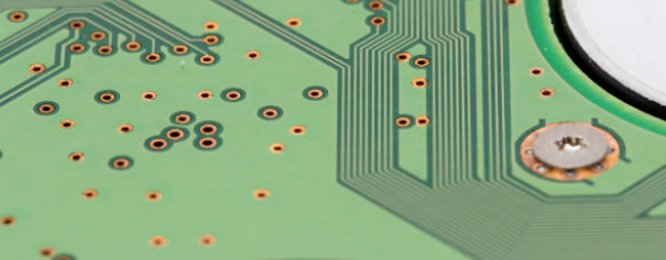
The annular ring is a perturbation of copper pad circumference that meets a PCB hole’s outer edge. Its most common use is to act as a foundation for soldering. it’s where through-hole components are put on the board so that the electrical connections between these components and the other devices on the board can be made. The ring not only provides a solid connection and good mechanical bolt between the lead of the component and the print circuit board but also creates an electrical connection between the PCB through the printed trace and the component.
Through-Hole

The through-hole refers to a drilled hole through the PCB trace substrate for mounting components or running conductive leads from one side of the board to the other that is copper-plated. Plenty through-hole leads are cut out through the holes drilled in a drill bits and soldered to the copper pads of both board sides. Bolt-holes are imminent, which refers to parts that require strong mechanical support and application where SMT attachment is not a preferable method.
In brief, the annular ring encircles the through-hole, offering a place for soldering components, and the through-hole itself holds component leads or layers additional copper. These two parts are, of course, essential in both PCB designers and assembly, especially when mixed methods are used, such as surface-mounted and other types of components, some of which have too much copper.
IPC Guidelines for the PCB Minimum Annular Ring
The IPC (Association Connecting Electronics Industries) is a standard created for various outline aspects of printed circuit board design and assembly, for instance, the minimum width of annular ring requirements. These are SMT-process requirements to achieve reliable soldering and connections, with consideration still being made for manufacturing possibilities. IPC-2221, The Generic Standard for Printed Board Design, has in it the advisory for a ring size which is based with the class of the PCB and the manufacturing processes.
The IPC-2221 standard typically suggests minimum annular ring sizes based on the following factors:
- Class of the PCB: IPC-2221 groups PCBs into 3 categories based on the purpose and user: Class 3 is mainly used for equipment where reliability is the most stringent; Class 2 is used for purposes like aerospace and aviation; and finally, Class 1 is used for commercial and industrial uses.
- Manufacturing processes: Annular ring sizes may be different from the minimum recommended value when using the standard through-hole plating, controlled impedance, or fine-pitch surface mount technology processes, respectively.
Common Problems of PCB Annular Rings
The annular rings of a printed circuit board may have several issues during the creation of the design, their manufacturing process, as well as when in accordance with assembly procedures. Such problems may spike up the robustness risks associated with the printed circuit board failure modes. Some common problems include:
Insufficient Annular Ring Size: If the annular ring size is too small, the problem may be that soldering will cause difficulties. Insufficient clearance between hole and pad of copper can cause soldered joints to be weak, unpredictable electrical connections, and even short circuits. This issue might be encountered with a design that is not prepared for the use of component-lead sizes, manufacturing limitations, or particular assembly routines.
Annular Ring Breakage: The annular limits of PCB manufacturing are vulnerable to breakages and damages along the production process, for instance, from sharp stress and aggressive handling. Fractures are likely to happen in instances of insufficient material strength, poor handling, and overstress from operations like drilling (drill bit) or plating operations.
Annular Ring Plating Defects: The defects that may arise during plating can range from voids to cracks or incomplete plating within the area. These imperfections may be the cause of the failure of solder joints and input lines for PCB conductivity. Surface and assembly defects are the most likely impairment factors caused by either poor process control, low-quality material, or improper preparation of surfaces.
Annular Ring Shorts: An unfortunate event in which the annular ring copper layer gets connected to traces as well as other conductive elements results when the copper plating of the annular ring area extends too close to those structures. Sporadic shorts might arise from improper design clearances, bad manufacturing, or spontaneous copper deposition during plating process stages.
Thermal Stress: Annular discs are sensitive to stress under thermal stress during operation, mostly because of high power dissipation or high thermostability requirements. Differential expansion of thermal stress can cause mechanical failure, such as delamination or fatigue damage at the solder joint, in the long run. Effective thermal management approaches, e.g., the selection of proper materials, including the substrate, or the incorporation of thermal vias, can help reduce these temperature surges.
Conclusion
In conclusion, PCB annular rings act as one of the main components influencing the reliability of soldering, mechanical strength, and electrical connection for through-hole components. e has to pay close attention to details such as annular ring size, either outer or inner circle, clearance, etc., during designing in order to avoid the most common difficulties being lack of dimension, breaking-off, plating defects, short circuits, and mechanical or thermal stress or mechanical stress and have a perfect width. Following industry standards, which involve entering designs for review and designing the printed circuit boards with manufacturers close by, is useful in solving these problems so as to ensure the general reliability and performance of printed circuit boards.

