Kick-start your journey in the PCB panel through the obstacles and rocks with our full guide, which includes the right techniques, expert hints, and best practices. Regardless of whether you’re a newbie or a veteran expert, our in-depth exploration will supply you with the knowledge required to grasp the intricacies of panel production, achieve higher yield, and subsequently reduce costs. By starting with the basics of paneling and even using advanced strategies, you can make yourself more than enough to achieve optimum PCB manufacturing results. Make your guides the roadmaps for your success that will come through mastering the art of PCB panels.
What Is A PCB Panel?
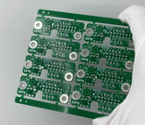
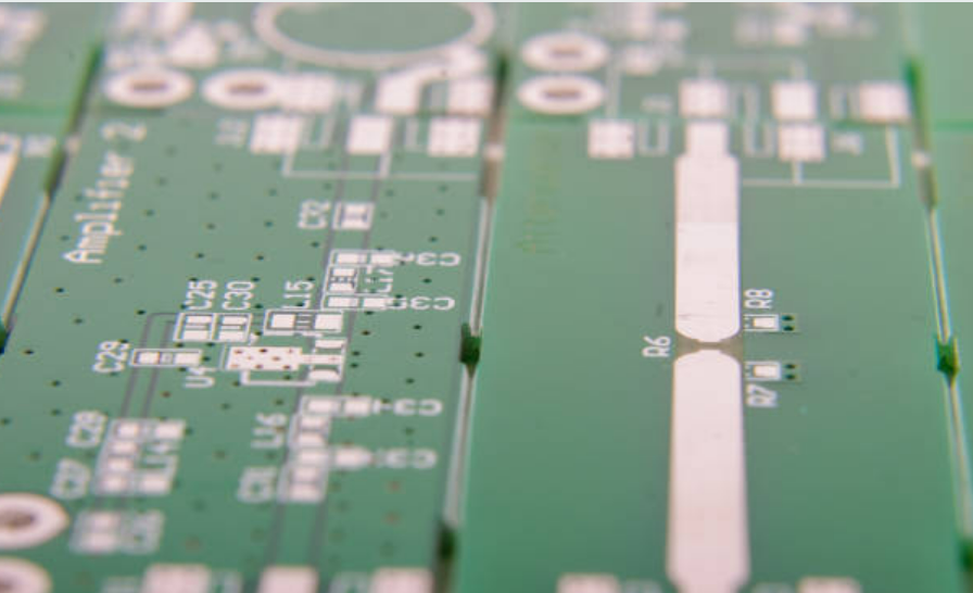
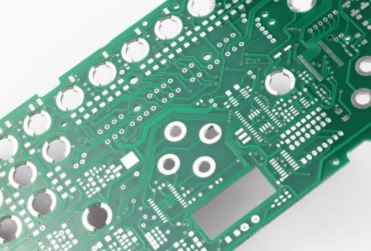
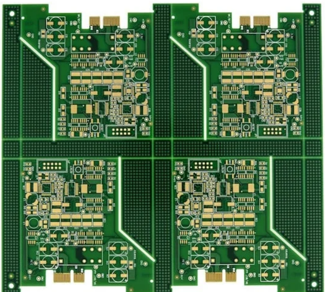
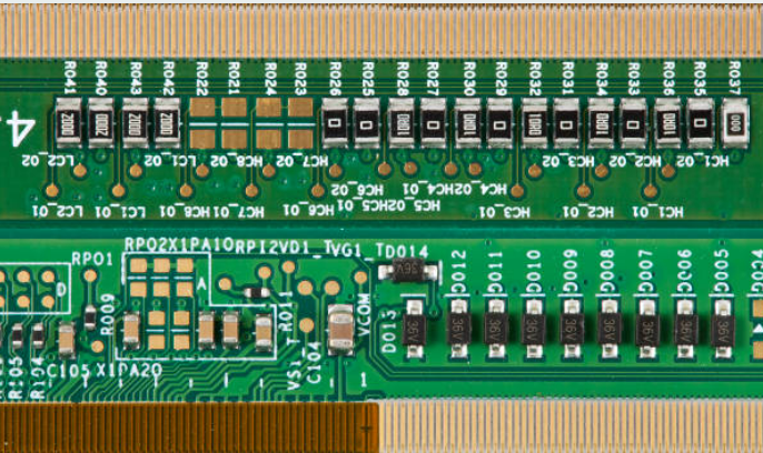
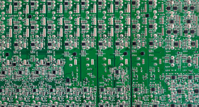
PCB panel, also known as a printed Board panel, is a group of PCBs mounted in a larger pattern to attain the benefit of production economy and ease of assembly. This method implies the production of several smaller PCBs at one time on a large circuit board surface, thus improving the efficiency of production and leading to a decrease in costs.
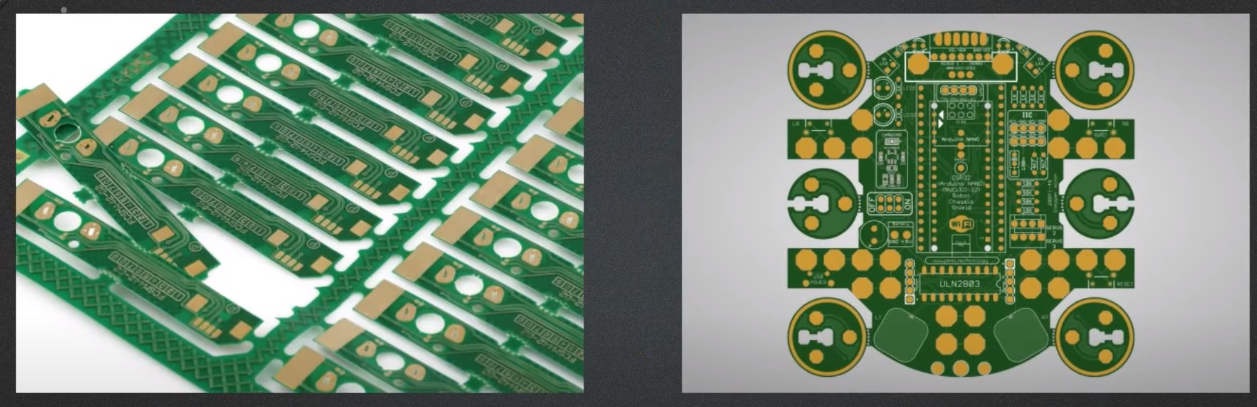
Oftentimes, individual unbounded circuit boards at the border or edge of the board panel are connected by breakaway tabs or routed outlines, which are separated during the assembly process. PCB panels are a vital part of the volume production operations, as they allow the manufacturers to optimize the process and further benefit from economies of scale.
Types of Printed Circuit Board Panel Design
Various types of printed circuit board (PCB) panel sizes unusual shapes and designs commonly utilized in manufacturing include:
1. Single-Board Panelization
Each PCB consists of only one side of the required circuit board that is further divided into smaller boards and double-sided boards to minimize costs in terms of space for the assembly and the test processes.
2. Panel Array
PCBs uniformly are prepared on a panel in a banana-like shape, using which both PCB production effectiveness and material-saving opportunities can be realized.
3. Step-and-Repeat Panelization
A repeated pattern within a single panel at a predetermined distance from solid tab panelization the next panel, with the gap between each instance held at its minimum is the mutual theme which ultimately brings material utilization and assembly efficiency levels to their best.
4. Tab-Routed Panelization
PCB entities are connected to each other through thin strips of excessive thickness—in fact, strips that prevent their removal from the front panel frame—during the production and testing stages. Lastly, the individual circuit completion is carried out by inserting the tab at the desired place and then snapping the tab’s extension together.
5. V-Groove Panelization
Wave patterns that are implemented along the borders of the board to signify every PCB group or individual board are put there, which helps to quickly identify the high turnover products.
6. Castellated Edge Panelization
PCBs separate the board edge and close-hole, through which the boards can be soldered, which raise the up-to-date designs diversity board size and complexity.
7. Scored Panelization
The PCBs have a description of lines with spaces between them, but the screw terms divide them. Therefore, after successful assembly, they can be cut apart easily. This method can be employed for a variety of product constructions, ranging from single boards to small to medium numbers of units.
8. Routed Panelization
PCB is separated from the panels with the help of full and tab routing panelization method of panelization machine installed in our facilities that have the capability of high precision and their operation can be modified to edge the routing process of irregular shapes of intricate designs.
9. Frame Panelization
PCB is hard-frame-inserted that can come with panel requirements an additional layer of support. This is used for panel requirements in the fields like complex layouts for large and/or complex devices.
10. Mixed-Design Panelization
Several Production Line PCB will be utilized in which the revised and variant product of should same panel will be produced at the same time.
Why PCB Panelization is Required?
PCB panelization is essential for several reasons:
- Efficiency in Manufacturing: Panelization technology makes possible having multiple PCBs to be produced at a time on one single panel. In this way, it increases the utilization of manufacturing equipment at a time and shortens production time.
- Material Optimization: Placing several PCB and individual circuit boards on a single sheet will reduce the amount of material being wasted, and it also means cost saving and environmental advantages.
- Ease of Handling: PCB panels provide easy handling during packing, testing, and transfer in cycle hence, there is a lower risk of damage leading to an improved process flow.
- Improved Assembly Accuracy: The panelization of PCB boards guarantees the expected level of preferred component alignment as well as spacing during assembly, making it possible to recover from errors and ultimately improve the product’s quality.
- Enhanced Testing Efficiency: PCB panels enable the usage of the batch testing technique, where multiple boards are tested at the same time, reducing the testing time and ensuring the parity of quality features across all boards.
- Cost Reduction: When producing individual PCBs for each board on a whole panel or a single panel, manufacturing costs are reduced per PCB that is typically lower in a large compared with a small scale of production.
- Support for Automated Processes: Due to the fact that panelized PCB’s are a perfect fit for automation of assembly and test equipment, subsequent production process is even faster and labor costs are even less.
Conclusively, PCB panelization becomes the backbone of modern electronic production to insure standard, affordable and high volume PCB production.
Advantages of PCB Panelization
PCB panelization offers several advantages in electronics manufacturing:
- Cost Efficiency: Altering between the panelization process of different boards allows reusing the manufacturing equipment to the maximum and results in lowering costs per PCB for the production.
- Optimized Production: Through the utilization of multi-Way technology (where many PCBs are simultaneously fabricated on a single panel), production time is decreased and throughput is increased, thus maximizing the manufacturing process efficiency.
- Improved Quality Control: To ensure consistent positioning and bond spacing during assembly, panelized PCBs are used in order to avoid installation errors and defects and to enhance the final product quality.
- Streamlined Assembly Process: The use of PCBs with pre-assembled panels or components is simple during assembly, testing and transportation. The unlikelihood of damage is also minimized with this system, and logistics is reduced to a minimum.
- Enhanced Testing Capabilities: Batch testing multiple boards mounted on the same panel polishes methods of quality checks, deploying dependable output and performance.
- Flexibility in Design: With panelization, a panel can contain either various PCB designs or manufactured products of the same type but of different shapes or other features. This allows for more persuasability in manufacturing as well as more options to accommodate different products and requirements.
- Scalability: PCB panelization helps in production scalability; manufacturers can adjust their volume of production anytime to the requirement without a grinding adjustment of the manufacturing’s process.
- Support for Automation: Panelized PCBs can be combined with automated assembly processes and thus can be subject to economy of scale, where the workload of humans is replaced with automatic procedures and labor costs declines.
- Environmental Benefits: Through PCB panelization, material waste is prevented and resource optimization is achieved. These enable sustainability initiatives and limit the environmental impact in the manufacturing process..
The PCB panelization in PCB manufacturing is a fundamental process that delivers numerous advantages in terms of product quality, speed of productions, and manufacturing processes cost savings.
PCB Panelization for Multiple Boards
Multiple PCB boards can be placed in a group at once with a panelized PCB board, thereby increasing the production efficiency. Here are some specific advantages of this approach:
- Cost Efficiency: Mass producing the same PCBs on a single substrate shortens the material cycle and increases the utilization rate of manufacturing equipment, thus keeps the production cost of one printed circuit per unit within low limit.
- Enhanced Production Efficiency: It is possible to create several boards side by side on a single panel thereby improving the production time substantially and increasing the throughput, which is especially valuable for large quantities of production.
- Consistent Quality: Panelization contributes to correctly accommodated boards with considertable spacing and alignment, reducing defects and defects, and consequently, the productity increases.
- Streamlined Assembly Process: All the steps in the process of assembling, checking and shipping the PCB with its panels are easier handling which add reliability and make logistics easy.
- Batch Testing: Board testing of stacked multiple boards on a single jig is a way to do the QA process efficiently which in turn ensures the reliability and performance of all boards in the stack.
- Flexibility in Design: Panelization facilitates combining several PCB designs, assembly of various product variants on a single panel, which may aid assorting production and satisying various product needs.
- Scalability: PCB panelization enables mass production and developing capacity where production can be scale up or down by changing in production level without significantly altering the manufacturing process.
- Support for Automation: Automated panelized PCBs have high affinity for high-speed production lines and help to lower production costs and to increase the productivity by cutting down the labor costs.
Basically, PCBs panelization for multiboards provide various advantages that ensure cost and time savings as well as high-quality production.
What are breakaway Rails in PCB Panel?
Breakaway rails or breakout rails, are parts of material used for isolating individual PCBs on a larger panel during a manufacturing process. This wiring attached to the edge-hanging components of the PCB helps to hold the edge of the board in place during board fabrication and assembly processes. When assembling, they take the PCBs off panel sizes by breaking or cutting along the rails. Breakaway rails provide several benefits in PCB manufacturing:
- Support and Stability: They support the overall stability of the PCB board, keeping it firmly in place throughout the fabrication, assembly, and handling processes, making any type of movement or shifting virtually impossible and hence a risk of destroying or misaligning it.
- Ease of Assembly: High rail breaking tools makes handling and moving the PCB’s inside the panels during the assembly procedure easier because they are glued together until ready to be broken.
- Efficient Production: Through using multiple PCBs on a panel that is connected, breakaway rail assembles production process that are effective by enabling batch PCB processing edge batching and lowering handling time
- Cost Savings: Saving a huge resource by applying the breakaway rails that work reduces the material waste of holding the PCBs by rails on the panel. This can lead to cost savings for rivals.
- Clean Separation: The humanizing task and easy detachment of the product PCBs after formation of the array will be insured by breakaway rails; smooth edges and less adjustment after production will be the result.
Technically speaking, breakaway rails basically find application in PCB panelization, mainly used to achieve high yields and cost-effective production of PCBs at the same time ensuring the quality of the PCBs.
IMPORTANT RULES THAT PCB PANELS SHOULD FOLLOW
Several important rules govern the design and assembly of PCB panels to ensure efficient manufacturing and high-quality results:
- Panelization Guidelines: Ensure that the industry standard rules on panelization are followed, such as spacing between PCBs, fixing fiducial markers, and provision for tooling holes used during fabrication.
- Component Placement: Place components onto a PCB panel using placement machines in order to obtain more effectively the assembly process outcomes and appropriately space components to get closer equipment and soldering expectancies.
- Clearances and Spacings: Preserving proper clearances and spacings amongst components, traces, and edges of the board is mandatory to prevent electrical interference, soldering bridge, and assembly errors.
- Signal Integrity: To ensure clean signal transmission, take into account the integrity issues, such as using minimal length of the signal traces, avoiding corners, and observing impedance control requirements.
- Thermal Management: Create a thermal relief, appropriate-size vias, and copper pours on the PCB design to enable speedy heat dissipation and avoid overheating of the components when in operation.
- Manufacturability: Give consideration to make-up panels, containment, and ease of assembly, as well as testability, handling, and inspection.
- Material Selection: Choose the right materials for your PCB panel, taking into account such specifications as the substrate type, its thickness, and the permissible properties of the laminate with respect to performance, service life, and cost.
- Panelization Method: Determine a specific panelization technique (e.g., tab routing, V-grooving, or scoring) based on batch, assembly method, and circuit board complexity.
- Quality Control: Applying rigorous quality control procedures right at the manufacturing process will permit the removal of detected defects or anomalies before PCB assembly and shipment.
- Compliance and Standards: Verify that the PCB panels are in accordance with applicable standards of the industry, including quality standards such as IPC standards and laws stipulating the design, production, and health and safety of electronic goods.
Through following the prescribed rules and regulations, it is possible to create smaller circuit boards that will be high-performing, reliable and manufacturable; at the same time, these jobs will cost less and the production will be shortened.
TECHNICAL CHALLENGES OF PCB PANELS
PCB panels, with their benefits, also have several technical issues that PCB designers, manufacturers, and assemblers should be aided to sort out. Some of these challenges include:
- Panelization Complexity: PCB design with multiple panels calls for vastly different arrangements of components within the given geometry, spacing, and positioning. It often proves laborious to juggle between standing waves that develop at individual boards, a problem that usually compounds in complex designs.
- Panelization Yield: Defective panelization can cause poor yield rates, resulting in solder bridging, misplacement of components, and electrical shorts being some of the reasons. Based on this, using panelization method and meticulous process control are key factors in achieving high yield.
- Manufacturing Constraints: The standard PCB panel sizes and material thicknesses, as well as the handling capability, might be limited during the PCB assembly and fabrication tools performance. Building panels that meet the certification standards without any constraints is contraption.
- Thermal Management: High-core PCB shelves with tightly placed components may not be enough to cool the components and cause thermal stress that damages the components due to heat. Correspondingly to these challenges thermal management strategies involving proper component selection, thermal vias and heatsinks are also crucial to tackle this problem.
- Component Placement and Routing: Using DRC (Design Rule Check), eliminating traces close together, connecting different layers, defining signal and power planes, and dealing with high-speed signals & RF circuits can be complicated tasks of board implementation for board designers, especially applying these rules in panelized PCBs design.
- Assembly and Handling: Panelized PCBs assembly, testing, and transportation need special handling to protect and install the modules one by one to be sure the latter will be aligned correctly. Assembly process management—the avoidance of solder defects as well as components damage—is the key factor to the issue of product quality
- Testing and Inspection: Verifying the test and performing superficially localized inspection of blind and buried vias, solder joint quality and shorts and opens can be quite a challenge when dealing with multilayer boards. Besides the employment of reliable testing and debugging systems, for instance, automated optical inspection and in-circuit testing methods are to be chosen.
- Cost and Lead Time: Although panelization can quicken the process and reduce the risk of human error, it may increase costs and lead times due to the high complexity of design, fabrication, and assembly processes. It is vital that the cost-effectiveness goal be considered in concert with quality and performance goals. When formulating an efficient design for PCB panelization, trade-off between the desired cost and performance level must be considered during different stages of the project.
Overcoming these technical issues requires the close collaboration of PCB designers, manufacturers and assembly line providers in developing new techniques and implementing panelized PCB jetages.
Conclusion
As a result, PCB panelization provides an alternative to streamline PCB manufacture by effectively grouping many of the individual PCBs into a single large panel. This technique increases the efficiency of products, reduces material reuse, and speeds up assembly and testing processes. On that account, design, production, and mounting of large panels must be carried out considering various aspects related to productivity, heat distribution, and component planification to handle the difficulty of low yield rates, heating, and distribution of components. Electronics assemblers can stay competitive in terms of producing PCB panels at a low cost and without sacrificing quality mastery by employing a complete knowledge of principles and elements of PCB panelization.