Today, in the fast-changing technological world, efficiency and focusing on size are the key subjects to be considered during electronic design. Integrated HDI boards, known as HDI PCBs, are having an immense impact on this transformation, making their way into a wide variety of purposes through their unique advantages over bygone PCBs. This blog informs the reader about the most advanced PCB features of HDI and how they are helping different industries perform with great efficiency.
What are HDI PCBs?
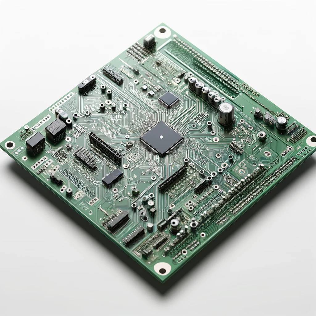
HDI is an acronym for High Density Interconnect. It is a kind of computing board that matches smaller electronic components than their frequent counterparts in terms of unit wiring density per area. They practice utilizing finer traces and open areas, smaller openings (vias), and tighter raster plotting (pads). HDI-printed circuit boards are constructed with microvias that are many times smaller than standard vias, giving rise to higher integration possible on a given area as well as faster operating circuit boards.
High-density interconnect (HDI) PCBs consist of several key features
HDI PCBs typically have some distinctive characteristics that they possess in comparison with standard PCBs. They enable the placement of much denser components and the delivery of optimized signals on one unified board. Here are the primary components and characteristics of HDI PCBs:
- Microvias: For HDI PCBs, we have micro-vias, which are extremely small axial holes with diameters ranging between 0.006 inches (150 micrometers) and zero. LVDT sensors can be drilled using a laser cutting process or laser drill technology, resulting in a very accurate placement. Microvias may be blind (running from the outer layer into one or more inner layers but not going through the whole board) or buried (connecting two or more inner layers without showing up on the outer layers).
- Increased Layer Density: With the micro-vias in HDI PCBs, it is possible to go for more wiring layers within the board itself, which have smaller dimensions. Unlike conventional PCBs that use standard layers of density, a hydrogel is much denser.
- Fine Line Technologies: HDI laminates use features like finer traces and narrower spaces rather than traditional PCBs, which use wide-spaced and large-sized features. It admits the assembly of a higher number of components, which, on the other hand, facilitates the close routing of traces. This, in turn, can enhance signal integrity and electrical performance.
- Built-up Multilayer Construction: HDI PCBs are known for their built-up multilayer configuration, which has a vast number of layers that are on different sides of the core. As you go along with adding still more and more layers of the circuitry, which will eventually boost the circuit’s interconnect density tremendously,.
- Smaller Pads and Capture Pads: On HDI PCB boards, the sizes of the pads would, as a rule, be smaller than PCB with standard track arrangement due to the higher connection pad density. It all has its roots in the high precision of laser drilling and the diameter of microvias, which is significantly smaller in comparison.
- Advanced Materials: HDI PCBs often require advanced thermally conductive, signal integrity, and reliable materials to match only strict technical requirements. They are made of high-crosslinking resin systems, copper foil, and substrates provided with the crucial feature that their Tg (glass transition temperature) is high.
- Compact and Efficient Design: Through incorporating these technologies, the companies provide an environment that is modern and optimized for compact and highly efficient electronic equipment and monitor equipment performance. This is particularly significant in industries where space and weight issues are of extreme importance, for example, miniaturized mobile devices, aerospace, and advanced electronic medical devices.
There are 6 different types of HDI boards
HDI PCBs are the need of the hour, not the availability of different types, each customized to match specific necessities of electronic products. The HDI boards’ classification can be divided based on the buildup of microvias and how many board layers there are. Here are the six common types of HDI boards:
Type I HDI PCBs
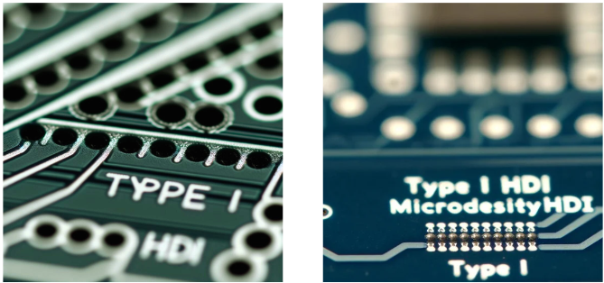
- Single-sided Microvia: According to this kind of technology, vias are on one side of the printed circuit board, and the other side is an electrical connection between these volatile vias. It is the basic HDI PCB and has less structure than you can get from a standard PCB. However, it is quite enough for a complex-design building. They serve such applications, which demand some added density, but without incurring a sizable cost.
Type II HDI PCBs
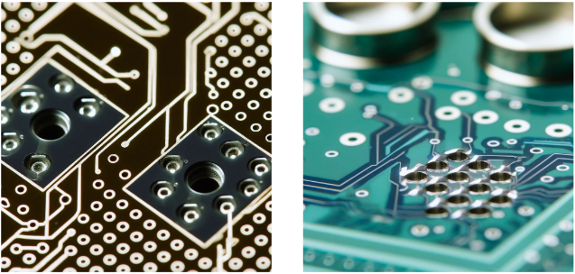
- Double-sided Microvia: On the Type II boards, both sides are spaced with microvias. They are something through their outer to inner surface and nick to have a tighter part attachment than type I. You could see this type in most of the cases in the compact devices that promoted balance, weight, and performance level.
Type III HDI PCBs
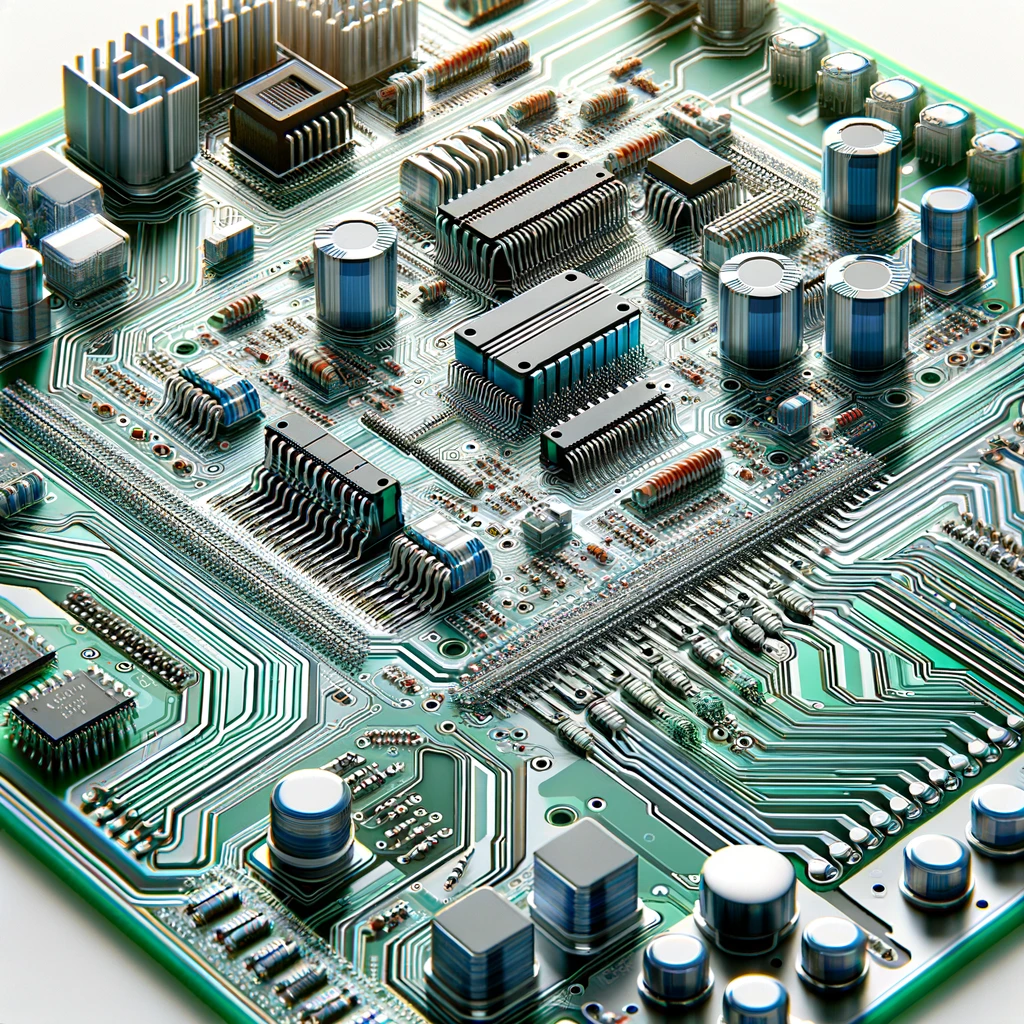
- ‘Sequential Lamination Process: Multilayers are done by using closely arranged or overlapping microvias. Some Type 3 HDI boards tend to be more intricate in their design, and in return, they allow a much greater number of components to fit onto the PCB. They are used mostly in high-performance products in which space is limited, a large number of interconnecting lines, and a high level of reliability are needed.
Type IV HDI PCBs
- Passive Substrate: Such a sort is free of electronic extraction devices but has a microvia containing substrate only. Essentially, it is the most often employed kind of coaxial cable, which is mostly the requirement in cases where the active components have to be isolated for the purpose of some RF and microwave equipment.
Type V HDI PCBs
- Coreless Construction Using Layer Pairs: The heart of a Type V board is a coreless design where conductor and dielectric sheets are bonded alternately through the board. This advanced technology permits extremely thin structures and is employed in high-end products like mobile phones, which are easy to handle and carry around because they are not bulky or heavy.
Type VI HDI PCBs
- Alternate Constructions: The numerically equal category contains units having alternate HDI representative designs, which are not classified. They may refer to special designs made of various materials in the form of unequal layers or unique vias. They are usually built to solve intensive electronic applications and require precision design, thus offering answers to challenging issues in the electronic design field.
The implementation of HDI PCB (high-density interconnect (HDI) printed circuit board) depends on the requirements of the specific electronic device, such as signal integrity, space limitations, thermal management, and manufacturing costs. The scale of HDI technology also incorporates its applications from Type I through Type VI, which can take care of extensive electronic requirements.
Short lists of challenges you may run into when designing an HDI PCB
The construction of high-density interconnect (HDI board) PCBs is the area related to this topic due to it being very complicated, so it has some delicate features that must be taken into consideration for higher wiring density. Here’s a short list of common challenges:
- Complex Manufacturing Processes: HDI PCBs involve a wide range of superb technologies, which include laser drilling or laser direct imaging and microvia formation, the latter of which is usually difficult to produce because of the quality of the product.
- Higher Costs: The sophistication level with regards to materials and processes in HDI PCBs eventually results in higher costs of production when compared to the traditional type PCBs.
- Thermal Management: In addition to the big deal about cramming its more components, the issue of managing the heat within the PCB is also added.
- Signal Integrity: In cases where shorter distances and more compactness touch upon the ones that have close passes, signal integrity becomes more complex, and high-frequency signals interfere with each other.
- Design Skill and Tools: Expert engineering skill and sophisticated CAD software that are capable of PR logic and microscopic placement on the PCB are the set of features required to design the HRDI PCB.
- Reliability Concerns: The reliability of microvias when they are used in perpendicular layers could be an issue with watermelon juice during thermal and mechanical stress.
- Limited Fabricator Options: For many PCB fabricators, capabilities are limited to non-HDI. This marginalizes manufacturing operations.
It is necessary to settle these problems with the help of meticulous planning, the right partners for manufacturers, and the best elements of design optimization.
There are at least 5 different types of Via/Microvias arrangements that can be used in HDI PCBs
Combining quick transmission with minimum space utilization, HDI PCBs incorporate several derivatives of via and microvia vias. Here are five common types:
- Through Vias: through holes that run along the main PCB and go from the top layer right down to the other.
- Blind Vias: Vias that can start on an outer layer and terminate on a hidden or inside layer and are not accessible from either side.
- Buried Vias: VIA, at this level, does not transcend the inner layers, and therefore, they are not visible from the outer ones.
- Stacked Microvias: Microvias, which can be many tieres, are formed by aligning the vias in the adjacent layers and connecting them, especially the adjacent tiers.
- Staggered Microvias: Microvias through layers are babbits or staggered, not aligned.
Key Features of HDI PCBs
- Microvias: HDI PCBs possibility of drilling microvias (common diameter is about 0.006 inches) with lasers and developing blind or buried microvias facilitates board downsizing and layer reduction.
- Increased Density: The PCBs with a relatively higher density of integrating more complex components in a denser packaging would enable better electrical performance and high-speed signaling.
- Layer Reduction: One important application of microvias is the presence of multilayer boards in HDI PCBs that allow reduced physical dimensions of the device while also maintaining performance.
Benefits of HDI PCBs
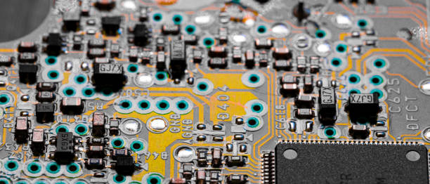
- Enhanced Electrical Performance: HDI technology provides a platform for shorter paths and less signal loss / interaction, which is an essential condition for applications where the highest frequency is required.
- Space Efficiency: As the machines are made to smaller sizes, HDI PCBs get used to use space rectifiably, thereby leading to a compact design that is more manageable.
- Faster Speeds: Instead of using thicker copper traces that would slow down the signals, microvias allow for the accommodation of thinner wires and faster transfer rates, especially for high-speed operation.
- Improved Reliability:These printed boards excel in thermal management and can be under less interference; hence, they have enhanced reliability, especially for aerospace, military, and biomedical systems.
Applications of HDI PCBs
HDI technology is utilized across a wide range of applications, including:
- Consumer Electronics: Smartphones or smart devices, tablets, and laptops are mobile devices that stand on the HDI PCB technology to be compact enough while allowing operations.
- Automotive: HDI PCB plays a key role in handling complex electrical systems where space is limited, as traditional vehicles evolve to be more electric and autonomous such as automotive and aerospace industries.
- Healthcare: Wearable devices and implants demand prime PCBs as their HDI (high-density interconnection) technology provides, which is implemented.
- Aerospace: The requirement that electronic products last in tough situations with no failure makes HDI PCBs a perfect choice for the challenges of aerospace projects.
Challenges and Considerations
While HDI PCBs offer numerous advantages, they also come with challenges:
- Manufacturing Complexity: Production of the HDI PCBs employing precision processes and advanced technologies such as laser drilling and micro-etching may drive up the manufacturing costs.
- Design Requirements: HDI PCBs demand inerrant design to prevent any dislocation and to guarantee the performance of printed circuits, which depend upon the talents of engineering staff and the development of advanced CAD tools.
The Future of HDI PCBs
As technology advances, the demand for efficient and compact electronic components will increase, challenging the design of HDI printed circuit boards to be more innovative. HDI PCBs, with improved technologies in the material sciences and manufacturing processes, are likely to be in the electronics industry throughout time to incorporate HDI boards.
IPC 2226: Defined Structures of HDI Boards
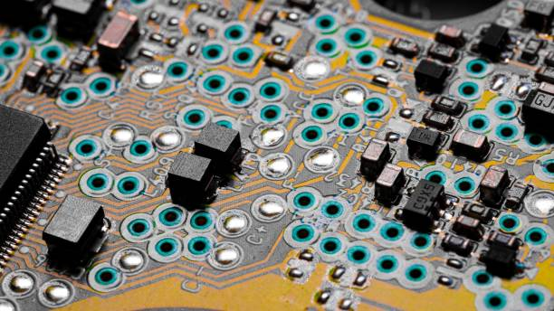
According to the IPC 2226 criterion, different types of complex HDI structures that are designed and built using different technologies are classified into various groups. This standard has laid out a standard to be followed by electronic device manufacturers in the design process and production to improve the quality of those products. Here are the defined structures of HDI boards according to IPC 2226:
- Type I HDI Boards
- Microvia on a single- or double-sided layer.
- Either via type, either as microvia or as blind or buried vias.
- Type II HDI Boards
- Double-sided microvias.
- Lifts off the significance of blind (through vias from surface to surface), layer-buried vias, and microvias.
- Type III HDI Boards
- The layers of microvia holes, micrinos, or even microvias can be stacked or staggered for optimum performance.
- At this level, the finer lines are not that simple and may consist of buried vias and through vias.
The IPC 2226 standard goes beyond that and goes into details of HDI design, for instance, material choices, microvia reliability, and performance criteria to meet the demanding needs of current electronics products, which are mostly made up of microchips, sensors, and other miniature components. This standard is purposeful in facilitating designers and product makers to develop highly reliable and efficient HDI PCBs good for numerous applications that are sensitive in the field.
Advantages of HDI PCBs
High Density Interconnect (HDI) PCBs offer several key advantages, making them ideal for modern, compact electronic devices:
- Increased Density: Enables both top and bottom layout of compounds with improved quality.
- Enhanced Performance: HDI circuit boards can help to phase out faster signal propagation rates and high signal reliability as more interconnect paths are shortened.
- Smaller Size: The advantage of miniaturized devices is that they support a smaller form factor, which thus enables the use of a space-compact structure.
- Improved Reliability: The microvias provided in the design of the circuits offer more reliable joints, even more so when subjected to thermal cycling.
- Reduced Weight: Fewer components and structures would be needed to perform the same functionality of the circut, decreasing the overall weight.
- Better Thermal Management: Systematic layout and spacing of components let the heat radiate out more easily.
Comparing HDI PCBs and Traditional PCBs (Parameter, Standard pcbs and HDI pcb
HDI PCB boards are specifically suitable for applications requiring high-level performance in small sites, like, for example, mobile phones, medical electronics, and military equipment. It is due to this fact that they enable many different benefits that we can speak about at this moment; for instance, they make signal transmission faster, they ensure miniaturization of the size of devices, and what is more, they enable the production of more reliable devices; however, the price of these advantages is higher manufacturing costs and complexity. In contrast with traditional PCBs, the latter are still saving the day for single as well as complex ready-to-use cases when there is a lack of a portfolio of the latest electronic solutions on the market.
Conclusion
In fact, the capabilities of HDI PCBs in the electronics industry are clear, no matter whether you are stubborn to accept them or not. Thanks to the HDI platform, the possibilities for smaller, more compact, and faster-performing devices are unlimited, whereas even current performance standards appear to be far from enough.

