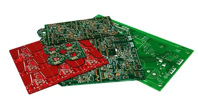
Although PCBs are the most widely used interface for connecting electronic components and mounting them on the device, they provide a durable and time-efficient platform for all devices. Manufacturing process of PCB is complicated, and a high level of accuracy must be ensured at all production stages. Let us walk you through the travel of PCB manufacturing from the idea to the finally done circuit board in this all inclusive guide.
What is the pcb fabrication process?
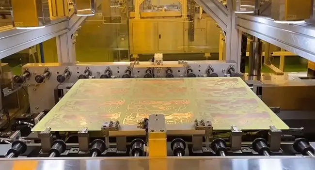
Fabrication of PCB consists of designing the board and converting the design into Gerber files, selecting a material, applying copper cladding, use of photoresist and imaging for making the pattern, etching of unnecessary copper, drilling holes, applying solder through the via, silk-screening, conducting electrical testing and spare cut-outs, and the application of final finishings.
Three main types of circuit boards
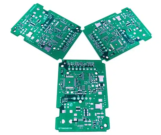
The three main types of circuit boards are:
Single-Sided PCB manufacturing process
Conductor layers are physicalize with one side of a non-conductive material, usually copper, which creates a proper conductive structure. While on PCB, components are placed with the copper (electrical conductor) layer, and connection is made by using the traces (auras) available on the board’s surface.
Double-Sided PCBs
These are made by either using conductive material on both sides of the substrate or combining nanowires with conductive particles. Components can be installed both equally to the right side and on the left side, and then connectors across layers are created using vias (holes that are coated with conductive material from the both sides).
Multilayer PCBs
Such structures, with their several stacked layers of conductive materials surrounded by insulating ones, have been found to be most suitable for coming up with devices characterized by their high performance and efficiency.
They facilitate more multi-layered designs and more components that can be put on covers. A via is used here to link up the layers. In multilayered PCBs an amount of layers could be from four to over thirty, but the four and the six layers boards are the most often used layers in general applications.
Printed circuit board Development
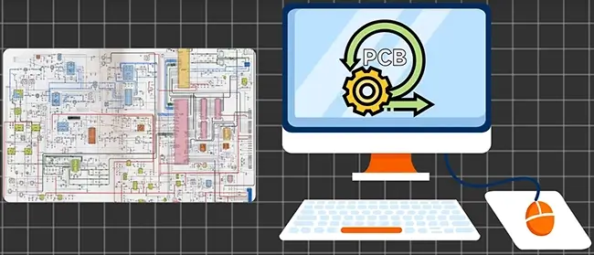
Printed circuit board (PCB) progress has finally advanced from primitive single-sided designs to modern multilayered and flexible constructs. Early manufacturing of PCBs occurred around a century ago, bearing in high technology developments especially in post-war period. The advent of the double-sided boards, holes plated through, and surface mount technology in the mid-20th century has enabled the creation of much smaller circuits that are also very complex.
Computer-Aided Design (CAD) based software was another significant achievement in the 1980s in the field of Printed Circuit Board design. Improvements in the recent times are screen printing and solder mask for HDI technology in which the size of vias and lines becomes smaller; flexible PCBs for bendable applications and the environmentally friendly manufacturing process.
Future intends to be technically linked to the new technologies, incorporating the 3D printing and nanotechnology as well as the increasing capabilities of HDI and flexible PCB.
PCB Manufacturing
PCB (printed circuit board) manufacturing involves designing the board, preparing all the materials that are required, etching away the excess copper to reveal the pattern of the circuit, drilling holes for the components, plating vias, applying a solder mask to protect the circuit and a silkscreen with labels onto the board, as well as other suitable tests for functionality.
This process can be simple or complicated, depending on the fact that it is one-sided, double-sided or more layers and more complex design, that is, they are additional stages.
PCB testing
PCB testing does not just include checking the functionality but also ensuring the reliability of the printed circuit board to achieve the nominal design specifications (NDS).
Such techniques comprise visual inspection, electrical tests – e.g. continuity and isolation checks – and more intricate methods like Automated Optical Inspection (AOI) and In-Circuit Testing (ICT) that can be used to identify any faults or problems earlier than the PCB design process moves to a finished product.
PCB Assembly
PCB assembly the process in which electronics components are mounted and soldered onto the circuit board which are to be called electronic devices.
This process may also comprise surface-mount technology (SMT) by putting the components directly onto the board, through-hole technology for insertion of the components into the drilled holes, and soldering which is used to lock the components in their place as well as to create the electrical connection. The traveled to PCB plating is tested for functionality respectively.
Standard PCB is made up of the following key parts
A standard PCB is typically made up of the following key parts:
Substrate layers of the pcb
Its core layer that can be fiberglass FR-4 to give it the structure and the insulation for the conductive circuitry, is the first component of a Printed circuit board assembly.
Copper Layer(s)
A fine copper foil matching the substrate is sandwiched between the thin plate of a lamination process. In a simple single-sided PCB there are just copper layers on one side of the pcbs. These copper layers may be present in double-sided PCBs or on multilayer PCBs in higher numbers.
Solder Mask
To avoid short circuit, a layer of a material is applied over copper. This layer also protects copper from corrosion that extended service would invoke. It also yields specific color to PCB which is what the PCBs are (generally green).
Silkscreen
Tin (silver oxide) will be placed on the build-up layer for positioning the sub-components, component numbers, and other critical information that facilitates assembly and troubleshooting.
Traces
The wire-traces that span copper layers signify billions of connections between individual components which are assembled on the printed circuit board.
Pads
You will also notice that your PCB has visible spots of copper where the components are soldered onto the board.
Vias
Tinned-hole that provides electrical connectivity between layers of a multi-layer pcb through a given reference.
Components
They are ordinary essential electronic components that include resistors, capacitors, and integrated circuits used on the printed circuit board (PCB), to create a whole workable electronic circuit.
Annular Rings
The circular rings lead to copper plating around the vias resolving the adhesion surface for soldering and to provide reliable electrical connection.
Component Leads
The metallic pins or leads of electronic components that are pierced through and provide electrical connections when soldered onto the PCB.
Edge Connectors
Metal pads or routes that forms both sides of the PCB which are utilized for connecting the board to other circuits or devices.
Plating process
The termination of some lines is made with a very thin layer of metal(usually gold or tin) which is applied to contact pads and vias to enhance the solderability and protect them from the corrosion.
Heat Sinks
Use a metal or other thermal conductor material on the board as well as on components to allow heat to be conducted away.
The PCB Fabrication Process
The PCB fabrication process involves several steps to turn a design into a physical printed circuit board:
- Design and Layout: Initially, CAD software is employed to draw an electronic circuit schematic and to provide the placement and tracing out of electric connections on the PCB.
- Gerber File Generation: Finally, the layout is transformed into Gerber files (a standard PCB fabricants’ tool) which are used to fabricate the boards.
- Material Selection and Preparation: The starting material for the PCB, typically a fiberglass laminate like FR-4, is called the fiberglass and is cut either by dry rout or CNC mill before being laminated or dissolvable in solvents. This material is what constructed the thing beneath which the deck stands on as well as it keeps the deck independent of outside influences of the weather.
- Copper Cladding: Those substrates have a very thin layer of copper laminated to the surface of the substrate. While the double-sided and multilayer PCBs are mostly referred to as having copper coating on both sides or multiple layers of the substrate.
- Photolithography: The hardening of the photoresist occurs by using it in a UV light as per the desired circuit pattern through a photomask. The exposed photoresist is turned into a negative photo in the developing process, showing the copper under the previous layer.
- Etching: The exposed copper is now chemically etched away leaving a circuit pattern imprinted only by the solidified and hardened photoresist.
- Drilling: Through drilling holes are being made into the board so that component leads and vias can be passed easily. Viase is a type of hole that provides electrical connection between different layers of the multilayer PCBs through the layers.
- Plating: The terminated holes are covered with copper or other conductive material in order to achieve electrical pathways form one end of the board to the other.
- Solder Mask Application: A solder mask is used to cover the entire board surface, thus the only part of the board that remains unmasked is pads and vias where the components will be soldered. This layer ensures that copper doesn’t corrode and the pads remain spaced, thereby preventing solder bridges.
- Silkscreen Printing: An elusive international consist to indicate component locations, and other info are printed on board by the process of silkscreen.
- Electrical Testing: The assembled board is inspected for continuity and shorts to eliminate any possible functions outside the designated purpose.
- Routing and Profiling: The electronic PCBs are cut out of the panel that they were manufactured on into their typical shape.
- Finishing: Finally the padding may be coated with surface finish which helps in protecting the parts from oxidation and improves the solderability as well.
How is a circuit board made?
The pattern of a circuit board is made via a process that involves creating the board layout design, putting a copper layer on the substrate, using light-sensitive materials to create the pattern, etching through the copper using the light-sensitive film hence cutting away traces until the board is ready, drilling hole and vias before they are being plated with a copper, and applying a solder mask to protect the board, then printing. The steps may be multiple for multilayer boards, and as per the application more steps might be needed.
Multi-layer printed circuit boards
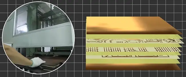
The Multi-layer printed circuit boards (PCBs) refer to the bluetops-degree circuit boards consisting of the 3 or more layers of slidable copper, separate by an insulating material. These layers are regularly enjoy laminates to form single contacting.
For function in items or devices where the free space is an issue or a more complex circuitry is necessary, there is use of multi-layer PCBs since they come with the ability to the circuitry with a higher density and interconnections.
We are used to that fact in devices like smartphones, desktop computers, and industrial equipment. Each thin echo excitations is imprinted with the circuit patterns to each layer being stacked and separated with insulating materials. This nonplace different method is performed by pressing and heating the stack to bond the layers together.
PCB holes and vias
In printed circuit boards (PCBs), holes and vias are crucial elements that serve different purposes:
Holes:
- Through-Hole: These are through holes drilled via the whole PCB application to finally mount the through-hole components. The four leads of the components are inserted into the indicated holes and eventually soldered on the opposite side.
- Mounting Holes: Hole types are in PCB are correspondent with the mounting technique to fix the PCB into a chassis or any enclosure. They are different from copper plated ones. This implies that their durability and resilience to harsh environmental conditions are top-notch.
Vias:
Through Vias are conductive way of a multiple layer PCB board connection. These pins are manufactured by making holes through the board and then later also having them covered with copper using the plating process. There are three main types of vias:
- Through-Hole Vias: The holes (these vias) that pass through all the layers of the PCB are circulating top layer to bottom layer to form a connection.
- Blind Vias: Vias here serve as a connector between the top layer or outer layer imaging surface and one or more of the inner layers ( inner and outer layers) but do not go to the opposite side of the board entirely. These types of devices are invisible when viewed from the other side of the PCB, therefore they are named “blind”.
- Buried Vias: These are the via through layers, two or more being connected but are isolated from the outer layers parts of the protein outer layer. These are buried in the PCB itself and look externally like one single unit.
Other Types of Holes:
- Counterbore/Countersink Holes: These are the pilot holes that are made with screws to be uniformly place in need for aesthetic purposes.
- Slot Holes: These are holes with a non-round cross-section that are used to mount the components which are not depressed into the PCB, or when there is need to provide flexibility during the assembly of the components.
PCB solder plating and solder resist
In PCB manufacturing, solder plating and solder resist are important processes:
- Solder Plating:A thin layer of wettability performance material, such as tin or tin-lead alloy, is put on the copper pads, and the lines. The immersion of the copper into nitric acid induces a plating thereof, shielding it from oxidation thus increasing solderability and providing the surface of choice for soldering the components.
- Solder Resist (Solder Mask): PCB getting coated all over by a soaked solution but restricted only on the areas where components will be soldered. On top of that the layer keeps the conductors from short circuits between solder bridges which are at a close distance to each other, and boards from environmental damages.
PCB silk screen
Whether it is the top side, bottom side or even both sides, PCB silk screen is a note of ink imprinted on the surface of the board and it represents a symbol of the origin of the PCB. The second layer is for labels, traces of the parts like resistor and some other thing like the title of the test points, polarity sign and and part number.
Silk screen will allow for the correct marking of the parts during mounting and failure diagnostic, therefore enabling the process to be more efficient while reducing the chances of error. “Screen table cloth” is a term that accrued from the fact that the process started by applying an original silk as a stencil material, but subsequently synthetic materials have been adopted more commonly.
PCB prototype
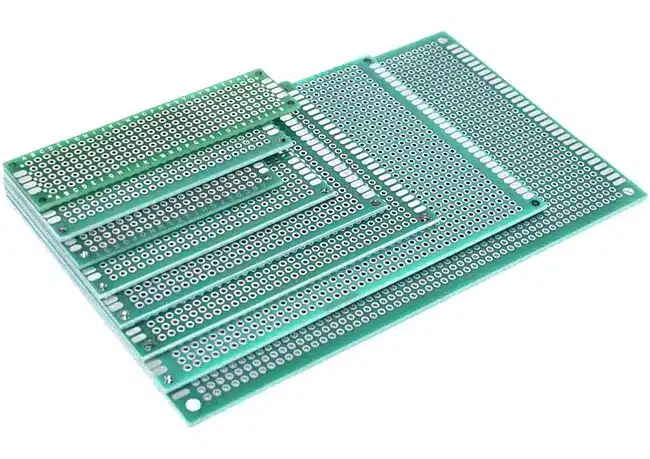
PCB prototype is a preliminary or initial sample or version of PCB, where designers implement this to test the logic and verity of the IC circuit configurations along with how the PCB would behave under various scenarios. Key features of a PCB prototype include:
- Rapid Testing: Enable designers to do iterations very fast, getting rid of design flaws and product deficiencies.
- Cost-Effective: In effect eliminates unwanted and time consuming errors that arise during mass production.
- Design Optimization: Facilitates continuous enhancements geared toward high-performance and production-compatible board output.
- Functional Verification: Provides that the paths in the circuit work towards meeting the expected specifications and needs.
- Short Lead Time: Shortening the prototyping phase is quite possible as in prototyping runs one could be quicker than in full production. Consequently, the development process is accelerated.
Printed Circuit Board services
Printed Circuit Board (PCB) Service includes an assorted variety of services from producing PCBs boards to consultancy services to entrepreneurs and private individuals so that they can develop and manufacture their own customized PCB manufacturing process.
These companies generally provide PCB design services, fabrication services, assembly services, testing services and a process of prototype production. PCB design service means developing the sheets and diagram of PCB and in accordance of the laid specifications and standard. The fabrication service is targeted to producing the PCB according to the existing design, incorporating technical capabilities and related materials. Services of assembly not only include mounting and soldering of components onto the PCB but also, mechanically or automatically.
A PCB is tested so as not to lead to malfunctioning and of course, poor quality. With the prototype services clients get a chance to check out a commonly small production batch of PCBs for the purposes of testing and validation before they begin mass production. Ultimately, PCB services takes pride to help electronic devices grow and undergo production processes, its specialists and support staff work daily to produce PCB designs on clients’ behalf.
Steps in the Manufacturing Process of Printed Circuit Boards
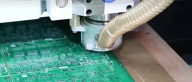
The process of manufacturing printed circuit boards (PCBs) includes a number of cumbersome but critical steps that ensure the final product is of high quality. Here are the main steps in the manufacturing process:
Design: It is intending to the design of the PCB layout using computer-aided design (CAD) software next. A layout is a description that involves arrangement of layers, routing traces, and placement of components.
Gerber File Generation: The design files are converted into a format that is used for further manufacturing known as Gerber files that contain information about the layers of circuit board manufacturing process, traces, pads, and so on. These files are utilized during production.
Material Selection: PCB substrate similar to FR-4 type of glass fiber-reinforced epoxy resin laminate material is chosen by manufacturers for the base material. In addition, copper foil layer are selected for the passage of the current due to their similar properties to the unwanted copper wire.
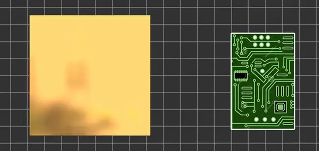
Board Preparation: Next, the thin copper foil gets laminated onto the substrate with a photo-sensitive and etching-resistant layer of polymer called photoresist. Then, the panel is cleaned and coated with a photoresist film.
Exposure and Development: A selective mask, also known as PCB, is put over the panel and light is applied through the mask using a UV source. D have attained a photoresist which when exposed would be developed showing pattern of the PCB.

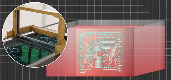
Etching: Finally, the panel goes through an etching process, in which the dissolvable masking copper is etched away delivering the traces of the mature copper shape.
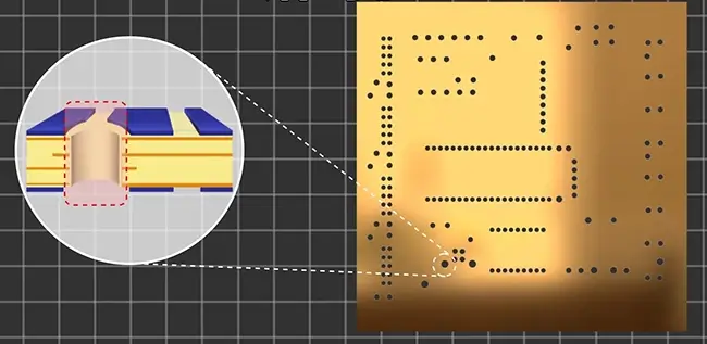
Drilling: Some holes are free of parts for bolting components into place or forming them into pairs. One of them is jumper to fill an empty gap and to make a circuit path. This way, holes are considered as component of multilayer PCBs and are plated with copper to create an electrical interconnection between components on a board.
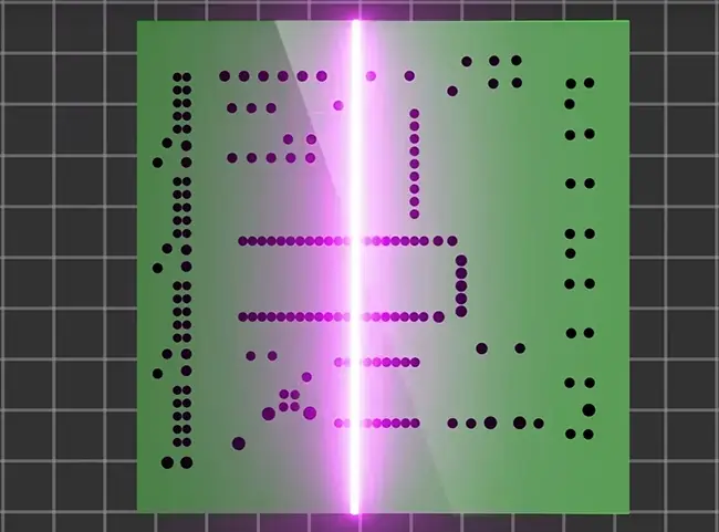
Solder Mask Application: The component is then coated with solder mask that covers the copper traces and prevents them from oxidizing, as well as stops the rising of solder bridges during assembly. Following the surface pretreatment, UV light is used to cure the solder mask.
Silkscreen Printing: Components designators, brands, logos and other markings made it using silk screen and ink. This also assists with the leads to the placement and identification of items.
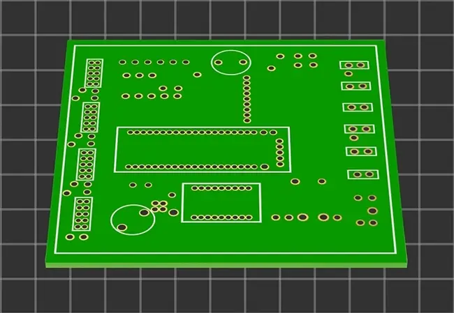
Surface Finish: A surface finishing is usually obtained for the exposed copper pads from the outside to improves solderability and protection against oxidation. On the other hand, typical surface layers are HASL, ENIG, and OSP.
Testing: After PCB is completed, it will has to go through different testing to see that it follows the given requirements and standards of quality. As a part of this, the electric tests, for example, may be included, as well as the visual inspection and functional tests.
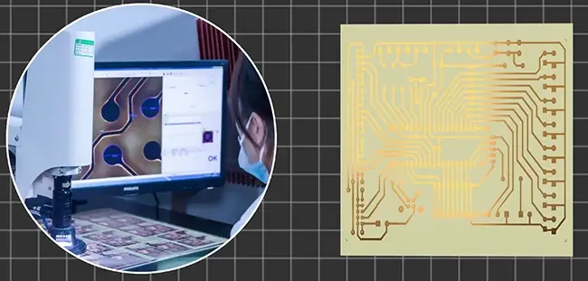
Assembly: Components may not be applied to the PCB yet when it passes testing. The configurations are aligned after components are placed. The components get assembled on the board either by using computerized equipment or manual assembly work, and then soldered.
Final Inspection: The PCB in the gathered state will have a final check done to make sure that all the components are positioned rightly, and also soldered in the right manner, while there are no defects or issues found.
Packaging and Shipping: Last step in the manufacture of PCBs is the packaging which is done as per customer needs and the devices are dispatched either to the end user or to the assembly site prior to use in electronic devices.
Conclusion
The PCB formation process is a complex one that requires the planning in advance, an ability to achieve the finest tolerances and the issue of assuring the device. Processing the concept from the start to final prospective of the circuit is the thing that matters the most to be sure that the PCB works like desired. In amidst of techtrends, PCB manufacturing goes through many changes too, so advanced electronics could be made.
Through understanding the intricacies of how printed circuit boards are made, we come to realize that they are not as underrated as their size might suggest but are actually tin plating, yet extremely powerful entities that sustain the advanced world that we live in.

