FLEXIBLE PCB
Flexible Order Quantities
We offer Rigid PCB production with no minimum order quantity, ensuring flexibility and cost-effectiveness for all project sizes.
Rapid Prototyping and Production
- Sample: 3-5 Days
- Mass production:8-10 Days
Advanced Layering and High Density
- Layers:4-32
- Versatile Layer Interconnectivity
Expert Technical Support
- One-on-one engineering services
- 24/7 Customer Service Online
- Flexible design
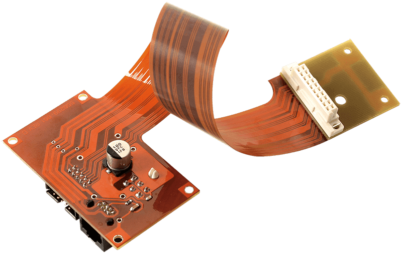
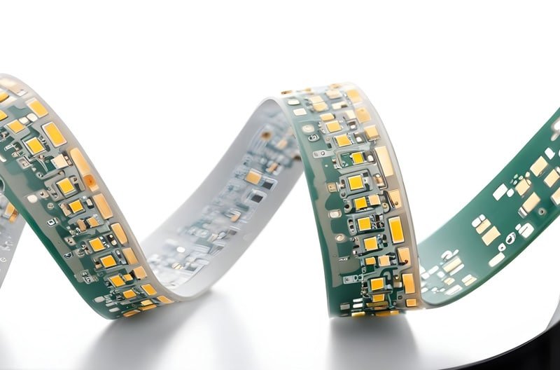
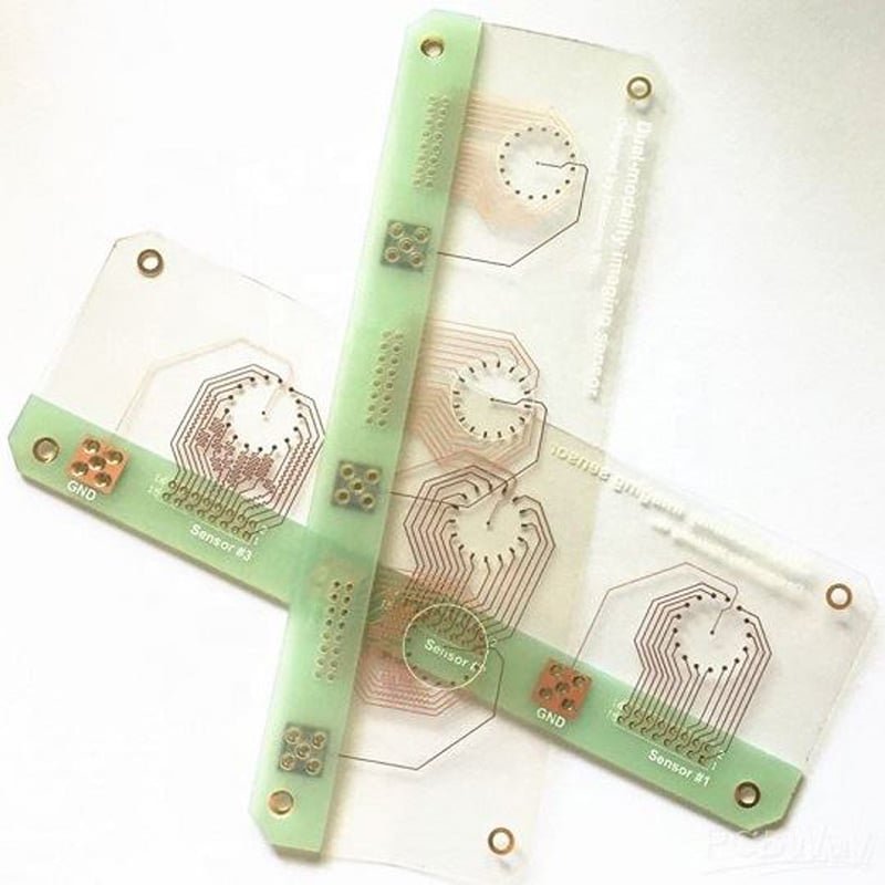
What is Flexible PCB
Flexible circuits, also known globally as flex circuits, flexible printed circuit boards, flex print, or Flexi-circuits, are part of the electronic interconnection family. They are made up of a thin insulating polymer film with attached conductive circuit patterns, usually covered by a thin polymer layer to protect the conductors. This technology has been used for electronic interconnections since the 1950s and has become a crucial interconnection method for producing many of today’s most advanced electronic devices.
High Temperature and High-Density Applications
Flex circuits are often made from polyimide or similar polymers, which dissipate heat more effectively than most rigid board materials. This allows flexible circuits to be used in challenging locations where heat could compromise the performance of a rigid board.
Flexible circuit boards can be engineered to withstand extreme temperatures, ranging from -200°C to 400°C, making them ideal for borehole measurements in the oil and gas industry.
Due to these conditions and the demand for compact, unobtrusive devices in industrial settings, flexible circuits are the preferred choice in many industrial sensor applications.
Their high-temperature resistance often pairs with strong chemical resistance and excellent durability against radiation and UV exposure. With the added ability to manage impedances in high-density designs, flexible circuits provide numerous advantages to manufacturers.
Comparison between the Poyester (PET) and Polymide(PI) material
The quality of a flex PCB is determined by its raw materials and stack-up. Based on market demand, three types of base materials are commonly used for flexible circuit boards: Polyester (PET), adhesive Polyimide (PI), and adhesiveless Polyimide (PI).
Are you familiar with the differences between PET and PI materials? If not, let’s explore them together now.
A reference chart is attached for your convenience, which should help you select the appropriate raw material based on the information provided below.
| Features | Polyester(PET) | Adhesive Polymide | Adhesiveless Polymide |
| Flexibility (2mm radius) | Bad | Good | Best |
| Tear strength | 800g | 500g | 500g |
| Strip strength in the air | 1050N/M | 1750N/M | 1225N/M |
| Eatching>=20% | BEST | Bad | Good |
| Working temperature | 80 | 85~165 | 105~200 |
| Chip | Bad | Good | Best |
The advantages and disadvantages of the PET and PI materials
| Material | Advantages | Disadvantages |
| PET | fewer production process; cheaper price; less lead time. | cannot pass through the soldering flow process; cannot work in high-temperature conditions. |
| PI(Polymide) | easily bend; can work in high-temperature conditions. | more expensive than PET |
Why Not Make All Circuit Boards Flexible?
Flexible circuit boards are highly versatile, but they are not intended to replace rigid circuit boards across all applications. Cost efficiency remains the primary barrier to adopting fully flexible circuit board designs in consumer products. Rigid circuit boards are generally more affordable to produce and install in standard automated high-volume production facilities.
For many innovative products, the ideal solution is a combination, using flexible circuitry where needed and solid, reliable rigid boards where possible to reduce manufacturing and assembly costs.
Some manufacturers use hybrid rigid-flex printed circuit boards to achieve this balance. This approach is common in devices like laptops and medical equipment, where rigid boards are connected by ribbon-like flexible circuits, combining the strengths of each board type to meet various engineering requirements.
PCBWay offers both flexible and rigid printed circuit boards for product manufacturers. Schedule a consultation with one of our sales representatives to determine whether your product prototype would benefit more from flexible or rigid circuit board designs.
Refer to the table below for PCBWay’s Flex PCB manufacturing capabilities.
| Item | Capability |
| Layer | 1-12 |
| Board thickness (without stiffener) | 4-40 mil |
| Tolerance of single layer | ±1.0 mil |
| Tolerance of double‐layer (≤12mil) | ± 1.2 mil |
| Tolerance of multi‐layer (≤12mil) | ± 1.2 mil |
| Tolerance of multi‐layer (12mil‐32mil) | ±5% |
| Tolerance of board thickness (including PI stiffener) | ±8% |
| Min. board size | 0.0788” *0.1576” (without bridge) 0.3152” * 0.3152” (with bridge) |
| Max. board size | 8.668” * 27.5” |
| Impedance control tolerance | ±5Ω (≤50Ω), ±7% (>50Ω) |
| Min. coverlay bridge | 6 mil |
| Min. bend radius of single layer | 3‐6 times of board thickness |
| Min. bend radius of double‐layer | 7‐10 times of board thickness |
| Min. bend radius of multi‐layer | 10‐15 times of board thickness |
| Min. mechanical drill hole | 4 mil |
| Inner Layer Trace / Space | 2 / 2 mil |
| Outer Layer Trace / Space | 2 / 2 mil |
| Solder mask color | Green / Black |
| Surface treatment | HASL, ENIG, ENEPIG, Electrolytic Nickel Gold, Soft gold, Hard gold, Immersion silver and OSP, Immersion tin |
| Laser accuracy (Routing) | ±2 mil |
| Punching accuracy (Routing) | ±2 mil ‐ ±6 mil |