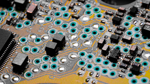
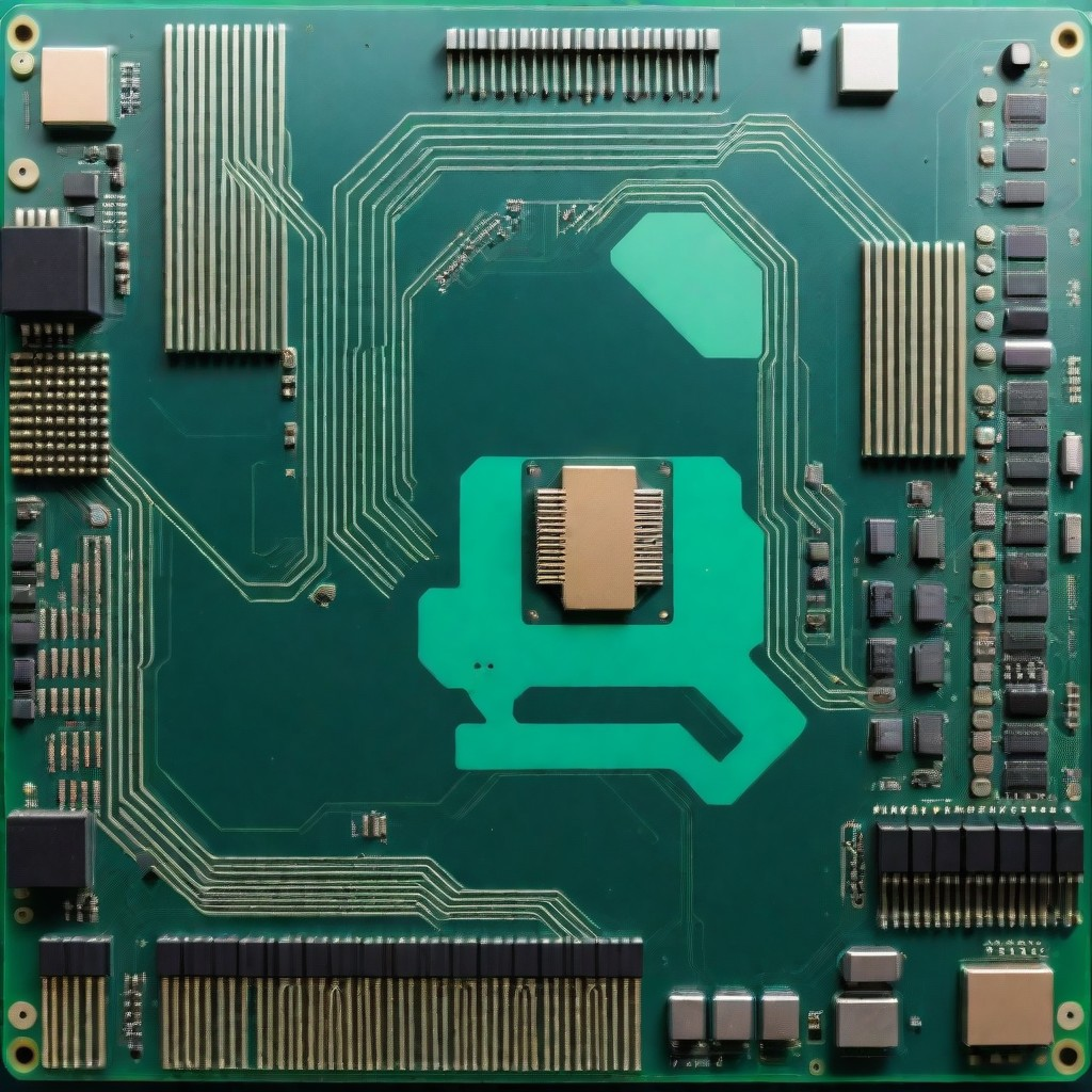
As PCBs (printed circuit boards) are capable of powering nearly every electronic device, from simple gadgets to tech equipment, they are recognized as the backbone of each industry. As technology complexity increases, the demand for high-performance PCB layout design is becoming standard not only in sophisticated products but also in consumer applications as well. The modelling pcb layout is a significant factor that will affect the feasibility, durability, and ease of manufacture of the final product.

Here, we are going to discuss some very effective PCB design tips as well as some rules that need to be followed in order to make the design more successful.
Top 5 printed circuit board designs
Here are the top five latest updates in printed circuit board (PCB) design as of 2024:
Integration of IoT and AI Technologies: The recent emergence of “Internet of Things” (IoT) together with “Artificial Intelligence” (AI) is actually massively evolving PCB technology. These developments achieve a higher level of operation and fine-tuning through the involvement of more automation, thus giving manufacturers a better chance to meet the demands for the highest quality at a lower production cost.

3D Printing of PCBs: 3D printing is changing the whole board production and design process because of the multitude of options it gives us, like the possibility to make complex shapes, eliminating much of the needed waste, and the facility of using more than just one material for them. This manufacturing technology not only gives the designers the opportunity to customize their creations and cut production costs, but it also accelerates the process of the production of these boards.

High-density interconnect (HDI) PCBs: The trend for high-density interconnect (HDI) PCBs makes for a more significant requirement that is inseparable from cutting-edge technology solutions in small-sized gadgets. Consequently, the condition that drives overall device performance comes up. HDI PCBs do especially well in smaller sizes, which is desirable for handheld devices and sophisticated gadgetry.
Advanced Material Use and CTE Management: With PCB evolution at flat levels, CTE has become an important parameter to avoid any warpage under temperature changes. With the appearance of new materials and processes, the exhausting capabilities and vulnerability of PCBs in different conditions improve.
Flex PCBs: The application styles of flexible PCBs grow on account of their hardness, and functionalities are intensified due to their compact size and attributes. This feature of additive manufacturing becomes obvious in consumer electronics, automotive, and defense applications, where one’s attention is always drawn to durability and performance.
These updates emphasize continuous innovations and improvements in the field of PCB design and note the industry’s efforts to incorporate new technologies and meet the growing advances in electronics.
There are several steps to take to ensure the design’s success before layout process

To ensure the success of a PCB design before starting the layout process, it’s important to follow several key steps:
Preparation of Schematics and Libraries
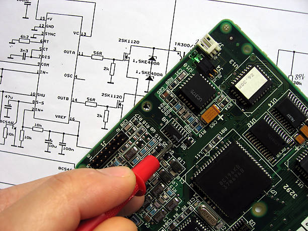
Before starting a layout, make sure that your schematics are complete and that all library elements are ready for use. During the schematic capture, be vigilant in verifying all the available components and their footprints within your PCB design software to prevent errors in the layout design stage.
Design Rule Configuration
Build up a description of all design rules and set boundaries according to your PCB requirements. These regulations will set specifications for widths of printed circuit board traces just like horizontal trace routing, pitch as well as vias details that are necessary to be met for manufacturing and performance.
Component Placement Strategy
Incorporate devices drawn from the schematic into your PCB software tool. Choose them correctly and strategically place them on the board in order to do so in such a way that there will be no signal interruptions during signal flow, as well as a minimal length of traces and the required clarity between the components for the signal integrity and thermal management of the device.
Planning the Power Delivery Network (PDN)
Create a robust power delivery network that can be guaranteed as a source of stable power everywhere. This involves location and designing decoupling capacitors strategically together, as well as ensuring the signal’s integrity more effectively through impactful power and groundplanes.
Critical Routing
Critical routing paths should be addressed first, especially for sensitive or high-frequency circuits; otherwise, chip yield will suffer. Employ techniques like differential pairing, trace length matching, and bending the trace to a smooth arc to bring about improvements in both the signal integrity and the electromagnetic interference.
Through particularizing each stage of the process and accounting for the fact that the PCB design should have everything done accurately so that the finalized PCB layout guidelines can be properly created, you can thereby significantly increase the chances that your design will be successful.
Guidelines for Placing PCB Components
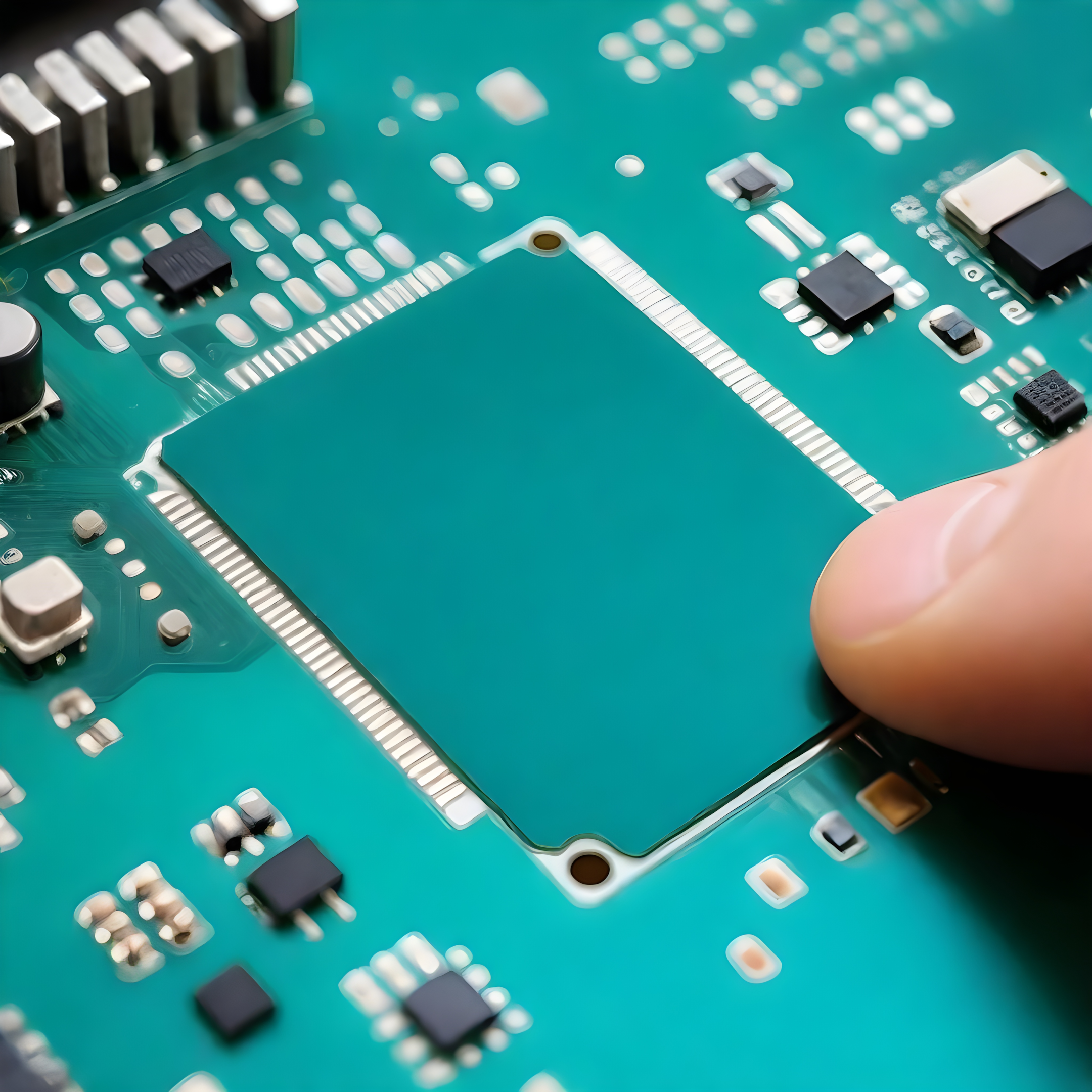
When it comes to placing components on a PCB, several guidelines should be considered to optimize the design for both functionality and manufacturability:
- Initial Planning and Placement: Start by drawing a simple map for your PCB designers so that you can determine the location of the components. This functionality allows for better use of space and reduces the disruptions that occur when analog and digital circuitry use the same signal lines to transmit data.
- Consider Component Size and Functionality: Start with the larger and more imperative devices (signal, power supply, etc.), as they typically have fixed areas. This then guarantees the comprehensibility of the complex data. Next, assemble these large and critical parts around which the minor and less important components will finish to fill in the rest of the network.
- Thermal Management: Ensure that components liable to heat are placed in a way that allows the removal of heat from their environment or from the system of the thermal relief pattern. Take care about the positioning of high-temperature parts, which can be very difficult and almost impossible to cool down if placed underneath other components.
- Minimize Signal Integrity Issues: Lengthen the components in sequence to keep signals short, and analog and digital signals should be avoided by crossing to prevent any problems. Apply the layouts of power and ground planes constructively to offer a good power supply and lower noise.
- Accessibility for Testing and Rework: Plan a configuration so that each part can be easily tested and repaired. Hence, all the important components would be exposed to manual testing and salvaging, requiring any future repairs.
- Automated Assembly Considerations: In the event that the board will be assembled automatically, ensure that you design test points and component seats in such a way that they will agree with the capabilities of the ICT or flying probe system.
These rules are going to, hence, incentivize the production of PCB designs that are not only functional but also cheaper, easier, and more maintainable. Take advantage of CAD (computer-aided design) systems and continually verify the rules and constraints while you are assembling the circuit board designs, thereby making sure that all the parameters are met for a successful PCB design.
PCB Design Layout Guidelines for Routing
A way of ensuring signal integrity, the reduction of electromagnetic interference (EMI), and the boosting of the integrated circuit signal performance is the necessity of the printed circuit board design layout guidelines for routing. Here are some key guidelines to consider:
- Maintain Short Trace Lengths: To decrease trace length is to mitigate signal degradation as well as EMI, with subsequent improvement of signal performance in general. This is very important, especially during signal transportation, due to the existence of long cables, which can lead to substantial signal quality problems.
- Controlled Impedance Routing: The leading emphasis is on managing the impedances of the signal traces at all times, in particular in the cases of speed designs. This computation is to design an adequate trace width and spacing based on the dielectric material or the plate thickness in order to meet the impedance requirements of the signal.
- Avoiding Crosstalk: Put the parallel tracks at a sufficient distance from each other to prevent crosstalk, especially for high-frequency data. There are also two other options for creating crosstalk reduction, namely routing perpendicular traces or using ground or power plane between adjacent signal layers.
- Use of Differential Pairs: For different returning signals, provide dual conductors with the same size and impedance. This acts as a barrier, which in turn makes the signal strong enough to prevent noise and its interference.
- Proper Grounding and Power Distribution: Introduce cathode-ray tubes, which are used for television, and comprehensive ground planes that would be disrupted by the loop, leading to better EMI performance. For delivering the power, wait for robust wires that are large enough to carry the current without voltage tension.
- Routing Around Obstacles: While mounting hole routing like surface mount components around obstacles as well as large component paths, you must select a distance-less path that protects the signals. Maintain connection integrity by keeping turns wider and rounder than those that lead to impedance discontinuities and signal reflection.
- Thermal Management in Routing: In addition to thermal management, top on the list of thermal concerns are the thermal effects of high-current traces either horizontal and vertical traces. Wider traces are good at preventing spikes in thermal load, while in some circumstances, thermal vias might be used to expend heat energy.
- Design Rule Check (DRC): Make sure you run the DRC on every PCB design to avoid any problems like scope violations, wrong trace width, or via problems before production. This will make sure the PCB is legitimate and holds up to all manufacturing requirements and operational controls.
If the designers follow the given patterns, they will be able to provide high-level functionality as well as reliability to the PCB. If it is a more detailed description and design methods that you are interested in, there are resources from Altium and Cadence that totally cover all the information you want.
Design Rules and Constraints
The design rules and constraints of PCB layout are the most important parameters that help guide the PCB design process and achieve two major purposes: one is to support normal functions, and the other is to make the board outline manufacturable with quality control process. The rules are principally defined by the fact that they address various parts of the structural layout, which include trace width, spacing, via sizes, pad sizes, and distance between the different elements. Here’s a breakdown of some key areas:
- Trace Width and Spacing: Minimum requirement for the electrical circuits and avoid short circuits to ensure proper current flow.
- Via Sizes and Types: Specification of conductive lines in trace via different layers, such as dimension and kinds (through-hole, blind, and buried).
- Component Placement and Spacing: Instructions for designing components with adequate room for assembly and operation within all preset boundaries, taking thermal expansion into account.
- Clearance from Board Edges: This ensures that there is a large enough buffer between the board’s components and traces and the board boundaries to avoid damage during manufacturing.
- Thermal Management: Guidelines on giving traces and pads the provision to keep the heat dissipation well-managed.
- High-Speed Design Considerations: Aimed at high-speed circuits, it consists of impedance control engineering and routing strategies that help to improve signal transmission.
- Silkscreen and Markings: Guidelines for positioning and number size to guarantee good readability and these components visual contact or soldering.
These guidelines will provide a structure to avoid production problems and also help the board match the quality standard. Devising software architecture usually ultimately incorporates the automatic tools to check these rules. The use of such instruments allows designers to eliminate problems before the production phase.
Top design software used to design a circuit board layout

Here’s a concise overview of some of the top PCB design software available in 2024:
Altium Designer: Sufficient for thick patterns on fast circuit boards, this layer offers good performance and comes with professional-grade integration tools as well.
OrCAD, produced by Cadenc, is equipped with the best automated verification and synthesis methods that simplify the design process for complex electronic and integrated circuits.
KiCad is a freeware, open-source package that is loved and widely used by both hobbyists and professionals due to it’s excellent functionality and active community base, which is always rooting for each other as they code.
DipTrace: The interface is easy to understand, and different packages are available that are fit for different user groups. Having a user-friendly UI teamed up with smart support assets is what keeps us on top.
Allegro PCB Designer is a strong Cadence software tool targeted at experienced users who may need complex pattern DRC capabilities and ECAD/MCAD linkage.
This is achieved by developing tools appropriate to different levels of proficiency and project complexity, and to this end, there must be a list for people right from beginners to professionals.
Popular PCB design software

Here’s a quick overview of popular PCB design software widely used in the industry:
- Altium Designer: A one-stop shop specializing in fast designs with advanced component libraries where users can access various engineering tools needed, thus making complex projects easier.
- OrCAD by Cadence: Besides, it has top simulation and schematic capture features, beloved by high-tech product-oriented designers.
- KiCad: It’s a DIY solution supported by a strong community, which is the best option for projects of any size if it’s up-to-date with the latest versions.
- Eagle (by Autodesk): A combination of schematic editor, PCB layout, and comprehensive library is provided and has been the highest-rated tool among hobbyists and designers to meet the ever-increasing demand for a simple tool.
- DipTrace: With its easy-to-use approach and wide range of pricing options, it has enthusiasts and professionals alike covered.
- Allegro PCB Designer: One item of the Cadence package intended for high-speed and high-density electronic products operating frequently in engineering where advanced implementations are required.
Every one of these tools aims to fulfill some or all design needs, from hobbyists to more complex multi-layer designs for industries.
PCB layout rules to follow in your design
Here are some essential PCB layout rules to follow in your design:
- Maintain Adequate Trace Width: Ensure that the cross-section of the conductors is large enough to carry the current power plane without excessive voltage drop and overheating.
- Control Impedance: Follow up the layout with controlled impedance traces for high-speed signals in order to maintain signal integrity. Write an outline for the given topic:
- Use decoupling capacitors: locate them near the power pins of ICs and thereby vary voltage as well as signal interference at higher frequencies.
- Manage Thermal Loads: Employ thermal vias that should be far from heat sources and keep temperature-sensitive parts in a safe zone.
- Keep Sensitive Traces Short: Shorten the signal transmitting range in the case of sensitive signals as a part of comprehensive measures to prevent electromagnetic interference and signal degradation.
- Separate Analog and Digital Grounds: Common ground plane should always be separate between analog and digital circuits to avoid digital noise affecting analog parts.
- Avoid Sharp Bends in Traces: This processing is done by 45-degree bends rather than 90-degree turns to minimize signal reflection and impedance variations.
- Plan for Testability: Provide samples for testing and constitute networks for diagnostics of these diseases, or introduce diagnostic kits.
- Consider Component Placement: Put components in positions that will help minimize areas of loop and which will reduce the strongest coupling, which often happens in high-speed circuitry.
- Follow Manufacturer Guidelines for DRC: DRC comparison with your manufacturer’s technical assistance should be part of your routines in order to avoid production problems.
Conclusion
Thus, given the changing face of PCB design, it always requires a deliberate strategy combining mentor practices with new technologies with the ultimate objective of producing both functionally and manufacturability-enhanced PCB. The design of a PCB depends on elaborate planning, thoughtful placement of the components, and an indication of the design standards (meeting electrical, heating, and mechanical needs). Innovations involving IoT integration and advanced materials are setting the course for (a) PCBs to ditch old playbooks, narrow down the difference in efficiency, and embrace new possibilities in the fast-modernized world. Utilizing the most up-to-date design software tools becomes a must, while there are more stringent processes to comply with as modern PCBs become more and more difficult to build. This way, by following the outlined regulations and making use of state-of-the-art technologies, we can accomplish both functional reliability and PCB projects.