Discover a comprehensive guide to excelling in EMI design with an emphasis on fundamental principles, progressive strategies and practical guidelines for creating EMC-friendly electronic devices. Get the upper-hand on noise control techniques as well as signal integrity by comprehending the intricacies of EMI management. Therefore, you are in a good position to offer optimal performance to your projects. The world of differential mode EMI design is constantly changing, adhering to new legal regulations and adopting new industry standards. Regarding the design and implementation of EMI, engineers and designers are seeking excellence. Expert advice is tailored to humans who strive for perfection; this is exactly what we are offering.
What is electromagnetic interference (EMI)?
EMI refers to electromagnetic interference. It is a form of interference that takes place when other devices or systems with their own electronic compartments being oscillated get influenced by electromagnetic radiation that might come from their close vicinity. EMI can be made in different ways, for instance, by electromagnetic fields, radio waves, or electrical conductivity. It becomes an important issue during consumer electronics’ design as it could interfere with most of the systems if electromagnetic disturbance is not either minimized or managed effectively. The EMI mitigation solutions include shielding, filtering, and grounding, as well as designing a PCB with care.
What are the sources of EMI?
Electromagnetic interference is a result of several sources. The hostile electromagnetic interferences generated internally and externally from the electronic circuitry of computing devices, or systems, are among the sources.
Here’s a breakdown of some common sources of EMI:
- Digital Circuitry: The transmission of high-speed digital signals such as those coming from microprocessors, FPGAs (Field-Programmable Gate Arrays), or digital buses (for example, SPI, I2C) could lead to high-power radio frequency and electromagnetic emissions given their pulsed nature and high frequencies.
- Power Electronics: Power supplies such as switch power supplies, voltage regulators, and other power electronics that inherently switch at high frequencies give rise to EMI due to their rapid switching operation. In unfortunate instances where power flows or regulators are not properly filtered, they harm the whole system.
- Clock Signals: Radiofrequency signals issued from clocks as a result of digital circuit synchronization are of particular interest because of their sharp edges for rising and falling levels. The ticking clock sounds in electronic systems are the main sources of EMI.
- Electromechanical Devices: Engines, relays, transformers, and other electromechanical devices can in turn produce EMI when they are switched on or in operation because of disturbances in electronic flow. Toward these ends, arcing contacts or magnetic fields that happen to be caused by the devices may also emit electromagnetic radiation.
- Cables and Connectors: Cables, connectors, and transmission lines may possess linear or bent antenna properties and give out electromagnetic radiation (EM). Unprotected cable or edged transmission lines with poor, if any, terminal terminations can lead to poorly shielded wiring systems and EMI susceptibility.
- Grounding Issues: Incorrect grounding practices may output ground loops and introduce noise sources into the system. Ground loops are situations where there are many paths in which current can flow around the ground connection to the equipment, which will generate disruptive electromagnetic interference.
- Environmental Factors: Factors like temperature changes, moisture levels, and electromagnetic fields from nearby equipment or machines can increase the level of electromagnetic interference that systems face.
- External Sources: The origin of EMI sources outside of human space has a wide range of sources: radio frequency interference (RFI) from nearby radio transmitters, wireless communication devices, power lines, lightning, and other electromagnetic sources outside the area.
Types of Electromagnetic Radiation and Interference
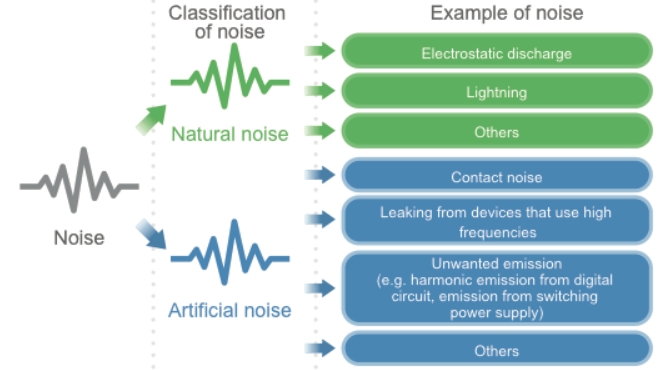
One of the major problems for wars and any form of military operations is electromagnetic interference (EMI), which is the general phenomenon relating to different types of electromagnetic radiation and harmful interference that can cause malfunctions (inter and intra) of various electronic components, other equipment, or information systems. Here are some common types of electromagnetic noise, radiation, and interference:
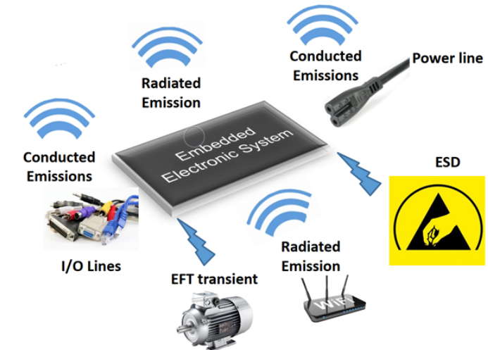
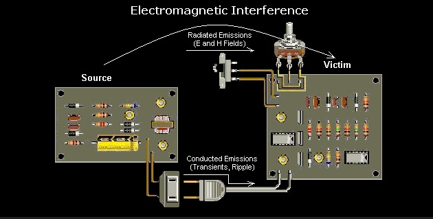
- Conducted Emissions:
- Government emissions could be traced through the conductive entry points of power lines, ground connections, and the signal traces printed on PCBs.
- Composed emissions count on semiconductor-based switches, a digital circuit, and communication lines with high-speed data lines.
- Radiated Emissions:
- Radiated emissions take place when electrical energy is converted into electromagnetic waves and reradiated to the environment through the medium of the air.
- Emission sources include conductive paths, PCB traces, antennas, and other conductive circuit elements on the PCB.
- Digital signals at high speeds and clock signals are the typical culprits for the emission of radiated signals.
- Common-Mode Interference:
- Common-mode interference results when undesired electromagnetic energy influences signal and return paths simultaneously in a transmission line.
- The issues may vary from asymmetry in the system to ground loops and external electromagnetic sources that can couple on the transmission line.
- Differential-Mode Interference:
- Differential pair interference occurs when differential-mode signals are found only on the signal transmission path of the transmission line.
- It can be generated by stubborn distribution differences, propagation between separate channels, or outside electromagnetic waves impacting the frequency.
- Radio Frequency Interference (RFI):
- RFI is radio frequency interference that could be anywhere from a few kilohertz to a few tens of gigahertz.
- RFI peaks cover RF transmitters, wireless communication devices aimed at RF devices, and almost all other contemporary electronic devices working within RF systems.
- Power Line Noise:
- Power line noise is an electromagnetic field that appears on power lines as a result of the switching of blowers, motors, or other similar equipment and units.
- The power line noise may be progressing through the conducting paths and transmitting in the form of an electromagnetic wave, which can effect sensitive electronic devices.
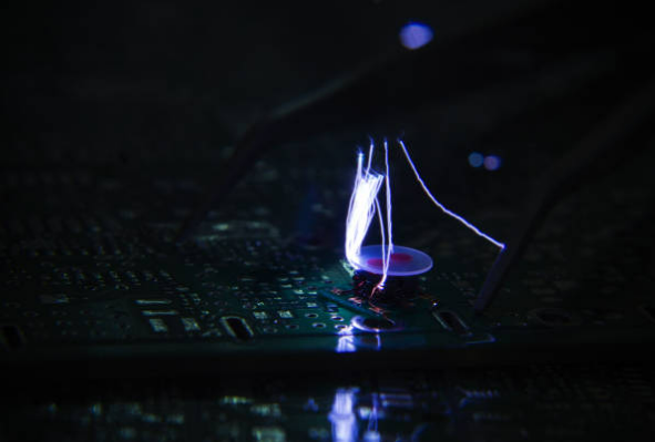
- Transient Interference:
- Transient interference—this term is also used to refer to electrical noise or voltage spikes, which are short-term disruptions of the electrical signal.
- Transients may be induced by not only lightning strokes but also ESD’s and operations on electrical circuits by switching.
- Harmonic Distortion:
- Harmonic distortion is the process whereby non-linear loads in the electrical system create harmonics at the fundamental grid frequency, causing interference.
- Operating at power factors creates voltage distortion and results in increased electromagnetic emissions from transmission and distribution systems.
What is the difference between EMI and EMC?
EMI (Electromagnetic Interference) and EMC (Electromagnetic Compatibility) are related concepts but differ in focus and scope.
EMI (Electromagnetic Interference):
- EMI simply denotes the undesired electromagnetic interference found with practically any electronic device or system and can affect the functioning of other nearby devices as well.
- It is therefore the emissions that disturb the working process at its core.
EMC (Electromagnetic Compatibility):
- To the same extent, EMC compliance comprises of conducted EMI and the capacity of an electronic system or device to be shielded or to be operating in its electromagnetic environment as planned.
- It symbolizes the wider principle of accessibility for electronic devices, such that they can comfortably interact or work without negatively affecting one another.
Design Guidelines for EMI and EMC Reduction in a PCB
Designing a PCB keeping in mind EMI reduction and ensuring EMC, that is, electro-magnet compatibility, is a task that follows several basic rules. Here’s a comprehensive list:
- Grounding and Layout:
- Employ proper grounding methods to keep the ground loops under control and get the currents’ low-impedance path. Therefore, protect the equipment from possible damage.
- Pick ground planes for analog and digital circuits that are isolated to avoid having a noise couple between them.
- Compare the part layout and lock path obstructions to reduce the probability of emissions and sensitivity.
- Component Placement:
- Placing the sensitive parts, correspondingly, on the high-speed or noisy components should be put off to create a less noisy environment for the place.
- Separate component groups having similar functions use PCB design software to mitigate signal trace and radiated emission.
- Signal Integrity:
- Working under controlled high-impedance routing for high-speed signals that inhibit signal reflections and EMI is a must.
- Apply termination techniques (series resistors, terminators) to stop signal ringing and overshoot that are generated by the signal source, and it might generate EMI if not performed properly.
- Power Distribution:
- Develop a noise-filtering network that operates at low frequency and has filter capacitors at the input for the active components, which should be installed close to them.
- Minimize power plane separation and try to solve the potential high-speed signal routing problem on this plane before the noise coupling process occurs.
- Shielding:
- Use shielding techniques such as enclosed cables, metal groundings, and conductive coatings as containment tools for electromagnetic radiation and interference prevention.
- Screen critical parts or sub-systems to keep them isolated from outside EMI sources.
- Filtering:
- Provide EMI filters at the main points of the circuit (they can be ferrite beads, capacitors, or inductors) to suppress high-frequency noises and avoid their propagation to the rest of the system.
- Filter along the common-mode noise in both signal lines and the power line by adding common-mode chokes.
- EMI-Robust PCB Design:
- Develop PCB traces with controlled impedance and correct path geometries (for example, differential signaling, length matching), aiming to limit emissions and susceptibility.
- Make use of ground-stitching vias in the circuit and along signal traces to provide a low-impedance return path and minimize radiation.
- Compliance Testing:
- During almost all of the design process, perform EMI/EMC testing with the purpose of detecting and resolving such problems as early as possible.
- Adhere to the EMC standards and regulations that are prevalent within your industry and fall under the jurisdiction of your geographical region.
- Environmental Considerations:
- Take, for example, the environment, where temperature, humidity, or electromagnetic fields from nearby equipment or machinery may be the cause of EMI/EMC while designing the system.
- Develop design solutions that have the capability to tolerate and mitigate the effects of the stated EMC factors.
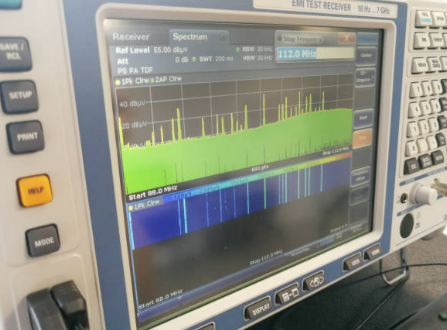
EMI/EMC Testing in a PCB Design
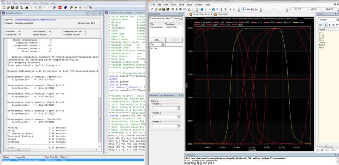
emissions, electromagnetic interference (EMI), and electromagnetic compatibility (EMC) of devices operating a circuit board are worth examining, so the final product will not violate government standards and the electrical system will do its work in the same environment as the chosen environment.
Here’s an overview of the testing process:
- Pre-compliance Testing:
- Before formal EMC certification, engineers frequently perform the pre-testing in the comfort of their offices. This is the performance of EMI measurement, and it is the responsibility of EMI measurement equipment to discover the emissions and susceptibility of PCB under controlled laboratory conditions.
- Pre-compliance testing is a powerful instrument that is used to indicate EMC problems early in the design process so that timely ambition for an effective design outcome can be realized.
- EMC Standards Compliance:
- PCB designs should conform to IP standards and local regulations that apply to the operating environment or targeted market. Composite EMC testing standards consist of CISPR (International Special Committee on Radio Interference) standards, FCC regulations, and CE directives (Conformité Européenne).
- EMC testing (electromagnetic compatibility testing) is conducted during the compliance check to grade the performance of the PCB in terms of radiation emission and interference immunity.
- Emissions Testing:
- Through emissions testing, the level of electromagnetic radiation emitted from the PCB during the transmission of the data through cables and connectors and during data transmission through the air is evaluated. Testing covers the frequency range to find out emission crests and to be sure their trends are in line with formal standards.
- Typical emissions sources from PCBs are such things as time signals, high-speed lines, and power supply circuits.
- Susceptibility Testing:
- The PCB’s susceptibility testing serves to determine its efficacy against external electromagnetic interference. The PCB under investigation is exposed to various types of electromagnetic fields, mainly emitted from the RF transmitters as well as the power lines, and has other sources to test its environmental capability.
- Performing the susceptibility tests saves the PCB of the hardware’s you would not want to work unreliably in your system of electromagnetic interferences.
- Test Setup:
- Conventionally, EMI/EMC testing employs test equipment that has to be specialized and is carried out in an anechoic chamber or a room shielded from external RF interference. The PCB goes through a series of tests on test equipment, including spectrum analyzers, oscilloscopes, and EMI receivers, to gather accurate emissions data.
- Transient platforms with signal generators, assist antennas, and others can be included while assembling the test setup.
- Documentation and Reporting:
- Conclusion results, which may include emission levels, susceptibility thresholds, and issues related to non-compliance, are submitted in a test report. The report brings out the PCB’s EMC testing and performance and goes with the given places that might need to be modified or improved to get compliance done.
- The documentation serves to get regulatory consent and product certification completed.
- Iterative Design Optimization:
- As per the test results and the EMC test results, the engineers work on improving the PCB design, and they iteratively, as long as they find the EMC issues, optimize the PCB design. Such a to-do list may comprise creating cover or absorbing measures, introducing EMI filters, optimizing routes, or improving the management of grounds and schematics.
- This design has been subjected to countless iterations. Only when EMC requirements are met can this process be halted.
How EMI and Electronic Devices Work Together
Electromagnetic Interference (EMI) and electronic devices are inseparable in that not only are electronic devices the source of EMI emissions, but they are also affected by EMI as well Devices like computers, phones, and so on, while running, produce electromagnetic fields & EMR that could make another nearby . For example, crowded with both high-voltage and high-speed digital circuits, microprocessors and FPGAs generate sharp edges in their signals, causing harmonics that are subsequently emitted as EMI. Also, there is radiated noise from electrical devices like switchgear and motor winding that may cause disturbances to the functioning of electronic equipment. On the contrary, device ignition systems that are electronic emit EMI (interference) into the environment from outside.
If electronic or computer equipment happens to be placed in the vicinity of electromagnetic fields coming from devices, power lines, or radio transmitters, they might actually experience malfunctions in the system, corruption of transmitted data, or even a complete malfunction. EMI becomes therefore a management problem in the good design of the electronics devices as well as in their operation to ensure proper functioning and reliability. Suppressing methods, adequate equipment, and EMI filters are all used to reduce the output, prevent the external interference of the electromagnetic field, maintain electromagnetic compatibility (EMC), and ensure the expected performance of the electronic devices in a normal environment.
What are the EMI/EMC Standards?
The electromagnetic interference (EMI) and electromagnetic compatibility (EMC) standards measure a device’s ability or system’s function based on possible or disruptive electromagnetic interference or interaction with other electronic components and systems in a shared operating environment in order to ensure that they continue working properly as intended in their intended electromagnetic environment. Here are some of the key EMI/EMC standards commonly referenced in various industries:
- CISPR Standards
- CISPR (International Special Committee on Radio Interference) standards are prepared by the IEC (International Electrotechnical Commission) for limiting and measuring methods of radio frequency allergy and immunity testing.
- CISPR 22 sets upper limits on and measurement options for ITEs (information technology equipment), within which computers and peripherals are included.
- CISPR 32: Prevents emissions from multimedia devices, e.g., televisions, set-top boxes, and audio/video equipment, by setting allowable emission limits and measurement methods.
- IEC Standards
- The International Electrotechnical Commission (IEC) stands to define norms and rules for product safety, performance, and compatibility.
- IEC 61000 series: Consists of various standards that regulate EMC parameters in different environments as well as the different kinds of devices, including protection against electromagnetic disturbances and the limits of emissions.
- IEC 60601-1-2: Specifies EMC requirements for medical electrical equipment and systems to guarantee protection of patients and equipment against hazards in medical environments.
- FCC Regulations
- The Federal Communications Commission (FCC) of the USA is responsible for emissions regulation, radio electromagnetics, and radio frequency interference prevention.
- Part 15: Establishes emission limits and compliance procedures or emission standards for intentional and unintentional radiators, like digital devices and peripherals.
- Part 18 is intended for industrial, scientific, and medical (ISM) devices with electromagnetic field-conducting devices and sets up limits to avoid radio service interference with licensed radio services.
- EN Standards
- The European Norm (EN) is similar as IEC standards, and they are implemented by EU member states.
- EN 55022: Matching CISPR 22 for lowering the maximum level for the discharg of emissions and giving guidelines how they must be measured.
- EN 55032: The same as CISPR 32, regarding emissions limits for multimedia equipment.
- MIL-STD Standards
- Military specifications (MIL-STD) are given out by different military entities so as to lay down the performance standards to be met by electronic gear that is used by the armed forces.
- MIL-STD-461: Providing technical requirements in the Military EMC standard for electronic military devices, such as emissions and susceptibility tests in electromagnetic environment of various types.
Conclusion
In summary, electromagnetic interference (EMI) design is indispensable for the safe and smooth running of electronic units and systems. By adopting proper grounding and shielding when planning the PCB layout design, selective component placement when designing the technology, and following other good EMI design practices, engineers can reduce both the radiation of electromagnetic energy and the electromagnetic susceptibility to interference of these components. This activity ensures the quality of electronic and electrical products, as well as reduces working costs for routine checks for unexpected failures, data loss, and meeting standards. The EMI design is a broad and complex task that calls for taking into account various related factors such as different types of emissions, surroundings, and the main standards of the country. By exercising the best practices and acknowledging the new technologies and regulations, the engineers will be able to prepare designs equipped with robust electromagnetic disturbance-compliant features that will match the high density of electromagnetic devices.