The Ultimate Guide to Printed Circuit Board Manufacturing: Everything You Need to Know
This paper gives an outline of the process of manufacturing the printed circuit board. The transformation of the design file into a physical board is illustrated step by step, with emphasis on the prepared design, the material of choice, and the precision in the process of fabricating. Among important stages explained by the document are layer stacking, drilling, etching, and how to finish. In addition, there is the application of solder masks and surface finishes to ensure protection and the ability of the PCB to achieve its function. The paper goes further to advise on some very important considerations, such as environmental impact and quality control at each stage of the process. PCB Manufacturing thus becomes the most perfect educational tool into the ideal machine for students and professionals who wish to understand the complexities of this technical process in the production of PCBs in churning out some high-quality output that conforms to standard technical requirements.
Expert Guide to PCB Layout Designing Techniques
The guide takes an extensive look at the PCB designs, and its centrality in the electronics industry is also stressed. The entire process is outlined from the initial analysis to the final testing stages with validation. The methodology highlighted underlines the significance of each step in shaping the product delivery in terms of functionality and reliability. The core principles like component placement, signal integrity, power distribution, and thermal management are explained, demonstrating how they play a significant role in the creation of an efficient PCB design. Furthermore, the article considers how design decisions affect ease of manufacturing and costs and reminds that developing such part of the process brings important financial benefits. The training manual also mentions key tools and software for PCB layout work as well as trends that affect the profession, e.g., small scale design and high-speed design. In this scholar-guide, you will find a lot of valuable information for electrical engineers and designers who want to optimize their PCB layout design to ensure that it is suitable for performance, reliability, and manufacturability.
Navigating Thru-Hole PCB Assembly: A Comprehensive Guide
The document is an ultimate resource which explains all the linear PCB assembly techniques, providing information about what is the best practice for each one of them and giving useful tips for execution a through-hole PCB assembly effectively. It cannels individuals with differing levels of experience from greenhorns to skilled workers, giving them knowlections about the manufacture of high class printed circuit boards. Guide highlights the significance of stress management, improving soldering skills and tackling most encountered challenges that one may experience when assembling a project. This resource is tightly related to teaching and learn through-hole PCB assembly and consequently becoming a useful part of both professionals’ and hobbyists’ product range who are keen on efficient product development and try to produce top-quality product.
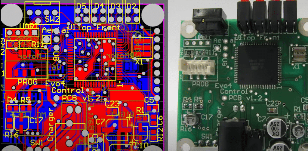
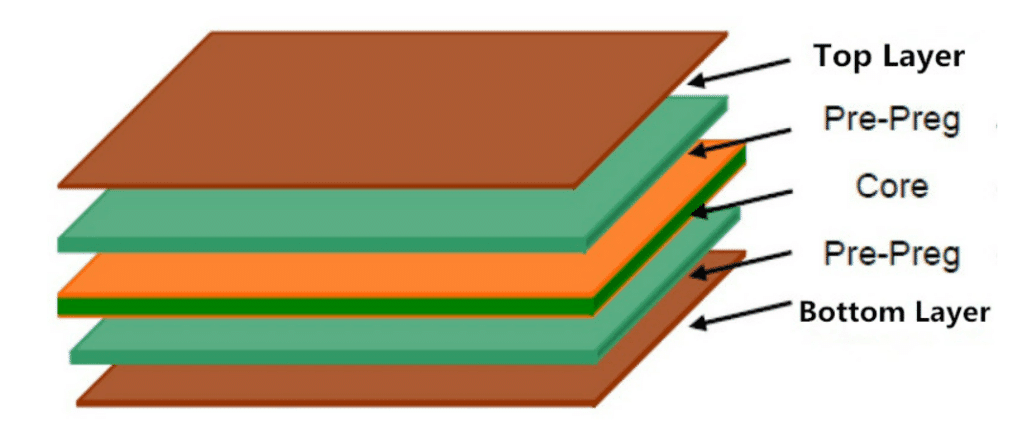
Understanding PCB Stack Up: A Comprehensive Guide to Multi-layer Circuit Board Design
The following paper is an in-depth guide for PCB stack-up design and includes the main information regarding the development of multi-layer printed circuit boards. The paper elaborates on the importance of stack-up design as one of the most important PCB design aspects that organizes different material layers in a PCB to ensure electrical features, signal integrity, and mechanical strength. This paper provides several kinds of PCB stack-ups that can be used, such as single-sided, double-sided, four-layer, multi-layer, rigid-flex, high-speed, and HDI stack-up, according to the special characteristics of the specific design. In addition, this guide covers the roles of various layers, such as signal layers, power and ground planes, and prepreg layers, in maintaining signal integrity, power distribution, and thermal management. The manuscript highlights guidelines, tips, and considerations for the design of high-speed boards, among which are impedance control, EMI management, and grounding, as well as the process of quality assurance contributing to reliable and efficient PCB production.
PCB Annular Rings Demystified: Everything You Need to Know
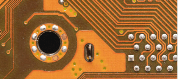
The annular rings are important aspects of PCB design, serving to create the copper area surrounding the holes that are drilled for purposes of soldering and electric connections. They elevate mechanical strength on the boards and ease reliability. The design of an annular ring is generally the art of creating an area around a hole on the pad, which is normally made by drilling a hole, addition of layers of copper, and removal of excess copper to take the form of the round pad. Annular rings are classified into Non-Plated Through Hole (NPTH), Plated Through Hole (PTH), Teardrop, Dogbone, and Tented Via; the different applications of the same. Annular ring size is a very important thing, and it will determine if soldering reliability and mechanical integrity will be upheld. IPC recommendations offer minimum annular ring size standards that determine manufacturability and performance. Some common issues on PCB that may degrade the reliability of the PCB are insufficient ring size, breakage, plating defects, and shorts. This design and meeting standards is the core component in the optimum functionality of PCBs.
Navigating PCB Panel: A Comprehensive Guide
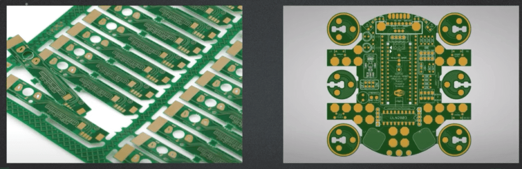
PCB panelization in electronics production is the step in which a greater number of smaller PCBs are fabricated simultaneously on a bigger board. It results in a more efficient process of production, with cost reduction and optimum use of materials. There are different techniques for panelization that match different kinds of needs in manufacturing, such as single-board, panel-array, and step-and-repeat. Panelization enhances testing and accuracy for handling, assembly, and test processes. It also simplifies material handling and is associated with better QC and repeatability. It also allows for automation that reduces labor costs. Some disadvantages are complexity, thermal management, and manufacturing costs. All these issues are to be overcome through the close collaboration of the designer with manufacturer and assembler to enable manufacture of efficient, cost-effective PCBs.
The Ultimate Guide to PCB Copper Thickness
In the article “The Ultimate Guide to PCB Copper Thickness,” the author elaborates on the importance of copper thickness in the construction of printed circuit boards. This is an important factor for functioning, performance, and life of the board. A guideline paper on the types of coppers used in PCB, such as ED copper and RA copper, and the scope of their application, is mentioned. The guideline goes further to explain how measurements of the copper weight and thickness are done and the factors that influence the choice of copper thickness, which has electrical and thermal requirements, manufacturing constraints, and cost. Again, it explains how the manufacturing process steps, which involve copper, in PCB are carried out and the reasons for the determination of the appropriate thickness to be able to optimize the performance of the board.
The Ultimate Guide to PCB Backdrill: Everything You Need to Know
The article “The Ultimate Guide to PCB Backdrill: Everything You Need to Know” discusses details of the very important process of backdrilling in the process of making printed circuit boards. It removes material from via stubs, allowing the minimization of crosstalk levels and impedance matching of the signals to be properly maintained, being most critical in high-speed and RF circuits. This guide carries many benefits that come with back drilling, among them improvement in signal integrity, enhancement in high-frequency performance, and optimization of the PCB layout. This can explain the design considerations, such as drill depth, minimum drill diameter, and stack-up considerations, because cooperation with the manufacturer is pivotal in terms of realization of precision and cost-effectiveness. It is for this reason that back drilling, with careful implementation and supporting strategies like impedance matching, does away with probable cons, including signal attenuation, to become a critical tool in today’s PCB design and manufacture.
A Comprehensive Guide to Designing a High-Performance 4-Layer PCB Stackup
What is a 4-layer PCB stackup?
4-layer PCB (printed circuit boards) is a kind of circuit board that made up of four different conductive layers interspersed with insulating layers. This circuit embedding process is performed in multiple layers and the stacking of all these different layers together results in a finished circuit board. In the 4-layer PCB, the conductive layers are nestled in a blob-like form and divided by insulating materials. It means that the chip-level PCB structure is more complicated and has a smaller millage than of the single- or double-layer ones. The additional layers offering more routes for the traces to follow can play a vital role, as this facilitates the reduction of signal interference, better distribution of power delivery and minimization of noise for which the overall performance is much better.
4-layer PCBs are seen in many types of electronics equipments, in particular those with complex circuitry like computers, mobile phones, and networks which need special circuits. They present the right complexity level versus cost while delivering generally good performances, which can be an advantage for many applications.
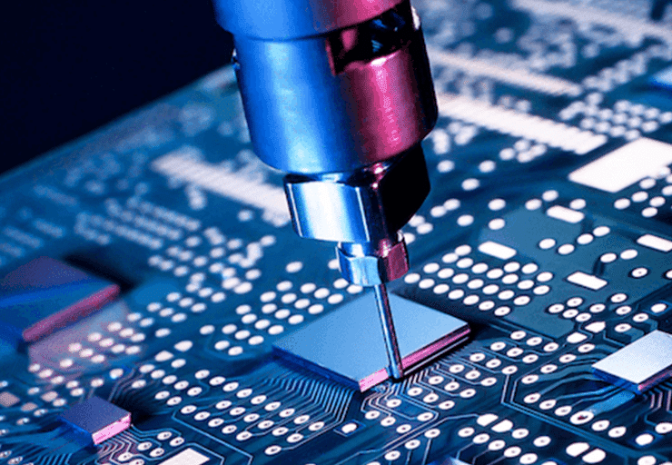
The Ultimate Guide to PCB Assembly: Everything You Need to Know
The guide offers a complete picture of the PCB assembly process, which is needed by people in the electronics industry, from novices to experts. It presents different assembly methods including Through-Hole Assembly (THA), Surface Mount Technology (SMT), and Mixed Technology Assembly and explains the role and usage of each method. The document explains the assembly process in a methodical way from the start to the finish, including the design and layout, the final inspection and testing stages. Besides, it talks about the various standards for assembling PCBs like IPC-A-610 and ISO 9001 which are responsible for the uniformity, quality and dependability in PCB production. Additionally, the guide stresses the importance of the Automated Optical Inspection (AOI) in the improvement of the manufacturing efficiency and quality of the product. This wide-ranging source gives the readers with the ability to understand and, consequently, to be involved in the PCB assembly process, thus, ensuring the high-quality production of electronic devices.