The Printed Circuit Board (PCB) drawings embody a guiding principle to all modern electronics device formations and production processes. The advanced technology, like phone and satellite, needs the detailed and accurate board drawing or board outline. The best printed board drawing makes it possible for the manufacturer to produce an efficient and highly functional product. Today, we’ll journey through the concept of PCB drawings and learn about those fundamental elements that could make your projects better with the help of owning a perfect understanding of such.
What are PCB Drawings?
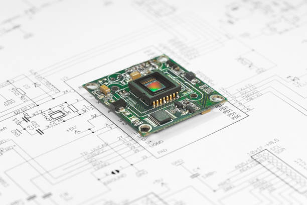
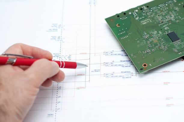
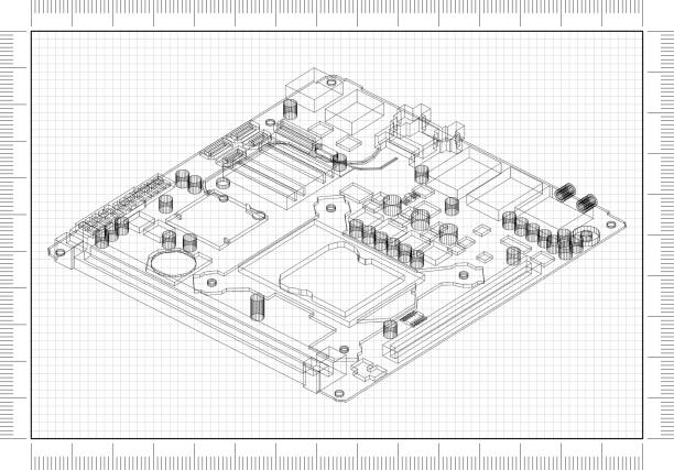
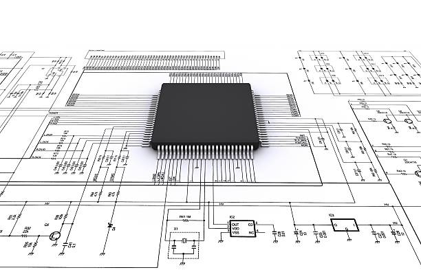
PCB layouts, also known as schematic thereof, are a set of particular renderings which consist in pictorial representation of electronic circuits of the assembly notes. The image sheds light on differing layers such as, location of components, signals and electricity paths, and mechanical curves respectively.
Key Components of PCB assembly drawing
These are the key components of pcb assembly drawings;
- Schematic Diagrams: A visual representation that involves elements and connections in the engineering process.
- Layer Stack-up: Usual link-up of copper and insulated layers to form a PCB’s architecture.
- Gerber Files: Standardized data that’s in anEXF file format that contains the copper traces, drill locations, and other crucial manufacturing data.
Importance of PCB Drawings

PCB drawing is a well structured documents containing more than simply the technical details; it acts the a connecting component between the theoretical world of theory and the demanding field of applications. Here’s why they are so important:
- Precision and Accuracy: They provide certainty that everything fits together correctly; as well, they closely examine the connections to prevent their damage and the resulting problems with functionality.
- Efficiency in Manufacturing: Accurate depictions will not cause incrunchment of errors as well as revision in manufacturing process, which may save time and costs.
- Ease of Troubleshooting: You will no longer guess during troubleshooting, where the fault is originating from with well-labeled drawings.
Best Practices for PCB Drawing Mastery
You can read the three best practices for your PCB assembly drawings and fabrication and assembly drawings;
- Start with a Clear Schematic: Ensure that your schematic diagram be error without committing mistake before you proceed to layout process. Here you will find the main source that will give you support during the procedure of design.
- Consider Manufacturing Constraints: Make sure that you know the requirements and capabilities of your PCB developer in details. The kind of traces and amount of space, and types of materials which are used are the ımportant components about one printed circuit board that will have influence over which PCB fabrication drawing method is utilized into the pcb fabrication notes.
- Utilize Advanced Software Tools: Try to explore the sophisticated electronic PCB design software such as Altium designer, Eagle, and KiCAD, which have incorporated the complexity management and accuracy enabling features.
- Perform Rigorous Testing: Implement various simulations (such as signal integrity, thermal analysis and electromagnetic compatibility) to accurately identify the problems in the design phase thereby enabling the issues to be solved in advance.
What are the types of pcb assembly drawings?
Good PCB assembly drawing come in several types, each serving different purposes in the PCB manufacturing process:
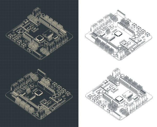
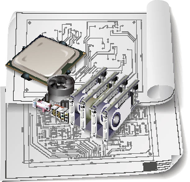
Assembly Drawing (Top and Bottom): Verify components placement on both top and bottom parts of the board.(Shows) It includes, besides, the kind of fasteners and those to be used, and the right marks to show the alignment.
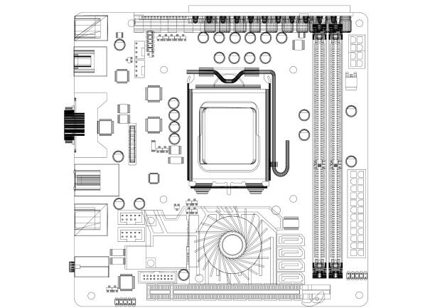
Fabrication Drawing: Shares any required specifications for making of PCB. It comprises measures, layer stack-ups, standards, and special handling instructions.
Schematic Diagram: Informs us about the circuit by means of its symbolic representation. In this procedure, it is important to investigate the electrical interactions and mechanisms.
Drill Drawing: Indicates the position, size, and type of the holes needed in the PCB, through a method including types of vias, through-hole, and non-plated holes.
This set of drawings creates a way like a puzzle to make a circuit board complete and fully assembled without jacking up all the electric and mechanical standards.
What is a fabrication drawing?
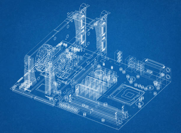
Fabrication drawing of a PCB (Printed Circuit Board) is also a detailed schematic that indicates each one of the necessary differentiating feature that is meant for its’ construction. Here are the specifications which contain the information of dimensions, the stack-up of the layers, the material types, hole sizes, and any plating or refining details. It also means to employ procedures and programming that enable the PCB to be produced accurately in accordance with the designer’s specifications.
Why Are PCB Assembly Drawings Important?
Assembly drawings for the Printed Circuit Board (PCB) is critical as it gives the workers proper instructions of how the component gets mounted on the board in the correct position and orientation hence ensuring that the assembly is accurate. They reduce mistake opportunities in the manufacturing phase, help in mocking up and removing of checkpoints, and keep on disparities in production and maintenance. Through these sketches, one constitutes a communication channel by connecting the designers with manufacturers, so that their innovative ideas appear in the final product.
Step-by-step Guide on Creating PCB Assembly Drawing

Here’s a concise step-by-step guide on creating a PCB assembly drawing:
- Design the Schematic: First of all it is necessary to develop the circuit schematic that explains the components and ways of the connections.
- Select PCB Design Software: Consider top PCB design software like Altium Designer, Eagle, or KiCAD which could help you to pursue your project.
- Layout the Board: Implementation of migration from schematic level to hardware layout, as demonstrated by the software that good routing of traces and components according to the circuits digital manuals.
- Define Layer Stack-Up: In your PCB board configure the configuration of Signal, Power, and Ground Layer, along with the desired insulating layer.
- Place Components: The components are to be situated so that they are constrained by heat, interference, and accessibility within the manufacturing and operations domain.
- Add Annotations: In column, label reference designators and working lead lines in order to facilitate the assembly process.
- Generate Gerber Files: Generate the Gerber files from the PCB layout which will be then given to the manufacturer for producing the photoresist plates of the PCB layers.
- Create Assembly Drawings: Build complete assembly drawings from the PCB design program with top and bottom layer, put all components on the drawings and notifies.
- Include Additional Details: Include any soldering pointers, component handling tips, or any special instructions about assembly.
- Review and Export: Do the checkup of the design and fix any errors or such things that are missing. Lastly, send it to the team of assembly in the appropriate format.
The guide which has helped us in providing quality PCB assembly drawings will expedite assembly and will reduce the time in the manufacturing process.
Conclusion
Being able to master PCB (printed circuit board) drawings certainly is a critical skill within the scope of professional electronics design whereby the end goal is really ensuring a high quality, efficient and, in the long run, fully functional electronic product. With adhering to the newest and the best standards, designers can not only provide a performing PCB but also can find solutions optimized for technology updates.
With the blueprints-to-bits transformation, we are securing the PC board layout design continual progress, resulting in increasingly smarter and more high-efficient electronic solutions. If you are a professional engineer or a beginner, you can access the future world of electronics by understanding PDF designs.