Learn the fundamental methods and clues of designing multi-layer PCBs which could be used for the best performance. Gain knowledge on material selection, layer stacking, routing techniques, and testing practices to achieve high-performance and robust PCB designs.
What is a Multilayer PCB?
A multilayer PCB (Printed Circuit Board) is one of many types of PCB, together with multiple layers of conductive traces and substrate-insulating material. However, it is more complicated than single inner layer-core PCB or double-layered PCB, which have conductive traces only on the inner layer core or the two layers. multilayer PCB claims to have conductive traces on multiple layers that are separated by the insulating materials. These layers are interconnected through vias, which are plated holes that facilitate the electrical flows passing from one layer to the next.
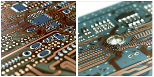
Multilayer PCBs are very popular in applications requiring sophisticated wiring, other PCB components and signal integrity. This is because they provide more routing lamp and flexibility compared to single- or multilayer PCB or double-sided PCB designs, thus allowing for greater design complexities and functions in a very small volume. Multilayer PCBs are a common feature of many electronic devices which include computers, smartphones, networking equipment, and medical devices that demand advanced PCN technology to cater to space constraints as well as performance requirements.
What are the Different Layers in a Multilayer PCB?
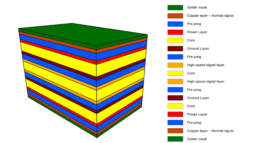
In multilayer PCBs, each inner layer is designed to cater to a specific purpose and each outer layer takes part in successful operation and functionality of the board as a whole. Here are the typical layers found in a multilayer PCB:
Top Layer
- The top layer is the outermost of the PCB and is packed with component placements, solder mask openings, and copper traces designed for signal routing. This is important for passing on signals and networking components that are present on the top side of the multilayer PCB.
Signal Layers
- Signal layers, together with ground and power planes, which are sandwiched between them and hold copper traces for interconnecting components, are named routing layers. This components are the pathway for the signals of the multilayer PCB and are essential for the maintenance of signal integrity and the reduction of EMI.
Ground Planes
- Ground planes are copper planes with high conductivity that serve as low-impedance return paths for signal currents and provide reference points for signal voltages at the same time. Grounding planes reduce interference noise, make the signal integrity better, and are also able to shield from EMI.
Power Planes
- Power planes are somehow like ground planes when they are not for carrying ground signals but just power supply voltage. They allocate the power to various elements across the conductive layers of the multilayer PCB, and they act as the return routes for power currents. Power planes are used in order to not allow voltage drops and to maintain constant power distribution through the entire board.
Internal Signal Layers
- Extra signal inner layers may be utilized when needed between power and ground planes and when routing requirements are complex or high-density design is requested. Such additional internal signal conduction layers also retain routing flexibility as well as signal integrity.
Prepreg Layers
- Prepreg are the layers made of fiberglass impregnated with epoxy resin that fill up the gap between the successive copper layers. They not only bond the cooper layers together when laminating but also give reliable mechanical power to PCB.
Core Layers
- Copper layers, which are first to be poured on the substrate (e.g., FR-4 fiberglass), make up the base structure in manufacturing multilayer boards. The lower level usually includes the inner signal layers, followed by ground planes and power planes.
Bottom Layer
- Just like the top layer, which has component placements, solder mask openings and copper traces for signal routing, the bottom layer also has the same elements. It functions as a base network for traces and devices at the bottom surface of PCB.
Through-hole Vias
- Thru-hole vias are plated holes that penetrate the exact multi layer board desired thickness and serve as single connection point between inner layers as well as various layers of the multilayer PCB. These conductive strips are used to forward power and command signals from one inner layer core to another, as well as ensure connectivity between the multilevel PCBs.
Blind and Buried Vias
- Blind vias and buried vias are just like the through-hole vias, but they penetrate only through the part of thickness of the PCB or are completely within the PCBs inner stacked layers, respectively. They permit signal to travel through them and reduce signal distortion and impedance variation.
What are the Factors to Consider When Choosing the Number of PCB Layers?
Selecting the number of traces for a printed circuit board (PCB) is the time PCB designers make decisions at least three layers from among various criteria. Here are the key factors to consider when determining the number of PCB layers:
- Complexity of the Circuit
- Evaluate the complexity of the circuit design, including the number of components, signal types (analog, digital, and high-speed), and routing conditions. Circuit designs that are more intricate and have a high component density, as well as complicated interconnections, may necessitate multi-layer board routing density for simple and effective circuit execution.
- Signal Integrity Requirements
- Assess the signal integrity needs of the PCB design, particularly HSI A/M applications. Likewise, the meeting of higher layer counts leads to the creation of dedicated top and bottom layers, ground planes, and power planes that perform the function of minimizing electromagnetic interference (EMI), crosstalk, and signal distortion.
- Power and Ground Distribution
- Determine the power distribution and ground connections compositions for the PCB. Another layer may be added as the power and ground networks, which can be used with dedicated power and ground planes to make a sound and stable power distribution, reduce noise, and improve EMI performance at the same time.
- Space Constraints
- Take account of the given dimensions and design of the PCB inside the final product. On the other hand, a higher number of layers will create additional space between the individual components. However, higher layer count will also add thickness to the whole board. Complex devices need additional layers, depending on the limits of their application in space.
- Cost Considerations
- Estimate the cost implications triggered by selecting a defined number of layers in the PCB. The second higher layer increases raw material costs, the work hours of numerous workers, and technology utilization related to drilling, plating, and lamination. Discuss the dilemma for deciding how to meet both the performance requirements and the budget constraints.
- Manufacturability
- Analyze the manufacturability of the given design with the particular number of layers chosen. Multilayer designs with a variety of complexities may need built-in steplike processes such as sequential lamination, micro-via components, and controlled impedance routing, and as a result of this, they can increase the number of production steps and thus the final cost.
- Thermal Management
- Take into account the thermal management problems in the PCB design for applications that either have high-power components or elevated operating temperatures. Substrate designs may be created using multiple connection points, such as for copper pours, thermal vias, and heatsinks, to enhance heat dissipation and heat transfer.
- EMI Considerations
- Characterize the effect that the PCB layout and IC count have on the electromagnetic compatibility and susceptibility of a system Layer counts above the present level generate BM’s and higher level of shielding and isolation between signal layers. It provides immunity from interference and meets EMC regulations.
Advantages and Disadvantages of Multilayer Printed Circuit Boards?
Multi-layer printed circuit board (PCB) comes with several pros and cons in the area of PCB technology compared to single-layer board or double-sided PCBs. Here are some of the key advantages and disadvantages:
Advantages:
- High Component Density
- Multi-layer PCBs are more efficient than single- or double-layer PCBs because they enable the placement of more components in the same space. He offers more area and liberty to design, so it is relatively easy, compared to classical PCBs, to handle circuits with high complexity and a larger number of components in limited space.
- Improved Signal Integrity
- Signal tracks, ground planes, and power planes of the multilayer PCBs tend to play a vital role in improving signal integrity by decreasing signal distortion, crosstalk, and electromagnetic interference. In this case, it is especially critical for the digital and RF/microwave modules.
- Enhanced Power Distribution
- Multi-layered PCBs as dedicated power planes are a perfect choice to provide stable power dissemination and low-impedance ways for power current flow. They cut down somewhat on voltage drops, electric and other distribution losses, and the overall effectiveness of the system.
- Reduced Electromagnetic Emissions
- The ground planes and signal isolation create layer spaces in multi-layer PCBs that have the EMI effect, and they diminish the EMI by the exact PCB components and by the outer devices. As a result, the radiated signals can travel in a more efficient path, and EMI and interference sensitivity can be minimized.
- Thermal Management
- Contrary to single- or double-sided boards, which provide suboptimal heat management, advanced multi-layer designs have copper pours, heatsinks, and thermal vias as an alternative for heat management. The heat generated by components is absorbed, which slightly increases the amount of heat passed to the area, thereby preventing it from overheating and improving its reliability.
- Design Flexibility
- Multilayer PCBs offer a designer more facility since they have a resource of several routing layers and signal planes. For example, a flexible multilayer PCB, where signal paths can be routed in a more efficient way, results in a large area and the accommodation of a wider range of functions, which directly leads to more optimal performance.
Disadvantages:
- Complexity and Cost
- Multi-layer PCBs are more difficult to design, manufacture, and assemble than single- and double-sided PCBs. Such patterns require the integration of complex assembly processes such as sequential lamination, blind/buried vias, and controlled-impedance routing, which can significantly decrease production and cost.
- Manufacturability Challenges
- The manufacturing process of multi-layered PCBs bring in many manufacturability issues, including registration errors, alignment problems, and higher defect proportion that have to be taken into account. Specialized apparatus and expertise must be in place in order for the weaving multi-layer PCBs to be flawlessly completed.
- Increased Layer Count
- Board thickness is often associated with increased complexity for multi-layer PCBs, which may not be either desirable or necessary in all applications. In case of equipment with electronic components manufacturing, there are those that do not need bigger and thicker PCBs because of their space or weight limitations.
- Testing and Debugging
- Multi-layer PBS testing and debugging are more complicated than single- or double-layer PCBs. Looking inside flow line layers and getting to the root of issues may necessitate the use of sophisticated instrumentation and procedures. Hence, the development cycle is likely to extend, while costs are expected to be higher.
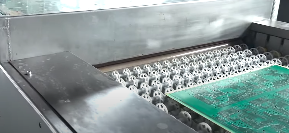
Conductive Material used in Multilayer PCBs
In multilayer PCBs, copper is the basic conduction-capable material for insulating two outer layers of the conductive traces. Copper is preferred for its high-quality electrical conductivity, soldering and welding properties, and low cost of production. How copper is used as the conductive material in multilayer PCBs
Copper Foil
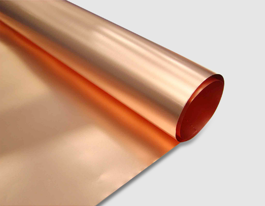
- Copper foil is the input material that will be used for the copper layer pattern. It usually comes in different thicknesses, and generally, these are the ones not bigger than 3 oz per square foot. Copper foil sheets with a higher copper thickness are used for high-power applications, while others are primarily used where additional copper thickness is a requirement from the design of conductive copper foil layers.
Layer Lamination
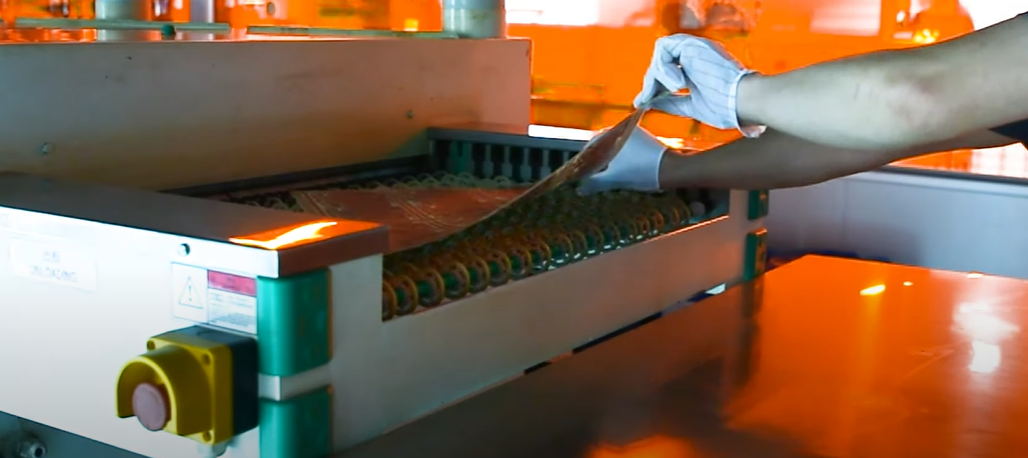
- A sheet of copper foil, which is the substrate material (usually FR-4 fiberglass), is laminated onto the same to create the conductive layers in a multilayer PCB stack-up. The copper foil is patterned through an adhesive layer and laminated to the substrate. The copper foil is generally chemically etched to create the desired circuit.
Inner and Outer Layers
- Copper foil is used as a two-sided conductor in inner and outer layers of the printed circuit board. Beneath the intermediate level of the PCB board structure, there are a myriad of inner layers that are completely buried within the PCB board stack-up. In sharp contrast, those on the topmost layer are exposed, with the pad of active and passive components, slots for solder mask, and copper traces, all visible on the exterior of the printed circuit board
Plating for Vias and Through-holes

- Plating copper vias and copper-plated holes is another application of copper, which serves as an electrical connection between different layers of the printed circuit board. Then, copper is applied to these holes through an electroplating process, which allows for the required connectivity and keeps them reliable.
Surface Finish
- Surface finishes on the copper traces that migrate to the outer layer of the printed circuit boards are plated to prevent oxidation and improve solderability. Any of HASL (Hot Air Solder Leveling), ENIG (Electroless Nickel Immersion Gold), or OSP (Organic Solderability Preservatives) can be used to give copper the final protection it needs by coating exposed copper with another metal or a material with protective layers very thinly.
Advantages of Multilayer PCBs over Single-Layer Alternatives
Multilayer (PCBs) designs possess some distinguishing advantages over single-layer designs because of their high capacity and functionality. Here are some key advantages of multilayer PCBs over single-layer alternatives:
- Higher Component Density
- Multilayer PCBs enable component packing to happen in a double amount in comparison to single-layer PCB. The designer may use multiple single-layer PCBs that can be divided into less assembled components with more complex designs within a quarter-smaller area.
- Improved Signal Integrity
- Dedicated layer of signals, ground plane layers, and power planes on multilayer PCBs are useful to increase signal integrity by minimizing signal disturbance, interference and electromotive interference (EMI). This is essential for digital and RF/microwave circuits, which work at high frequency.
- Enhanced Power Distribution
- multilayer PCB with dedicated power layers ensures stable power distribution and low impedance path to the power moiety. Therefore, it prevents voltage drops from the transformers, contributes to the lowering of power distribution losses and increases energy efficiency as a whole.
- Better Thermal Management
- Multilayer PCB substances with copper pours, thermal vias, and heatsinks offer more beneficial heat management than single-sided PCBs. Such devices tone down the heat better than cooling efforts for components; hence, performance is improved and overheating is prevented.
- Design Flexibility
- Multilayer PCBs provide more design flexibility because this variety offers multiple routing layers and signal plane. Designers can process signals with low wiring overhead and create designs that can accommodate the most challenging printed circuit board (PCB) designs or fit them in a small package.
- Reduced Electromagnetic Emissions
- Multilayer boards, including ground planes and signal isolation, are one of the means through which electromagnetic emissions will be minimized and propagated both within the PCB and to external devices. This greatly decreases radiation harmonic content, which results in EMC and higher immunity to interference.
- Space Savings
- The multilayer PCBs provide so much convenience in terms of space and compactness because the multiple circuits of single- or double-layer boards can all be merged and fit into a single multilayer board. It, thus, lowers the device’s carrying size as well as their weight, which in turn makes them more transportable and simple to integrate into many uses.
- Manufacturability
- Although multilayer PCBs are complex and expensive for fabrication, the new technologies in PCB manufacturing have made them more affordable. Such elaborated tools and experience are needed and sometimes might be the biggest difficulty in the epoch, but the benefits usually outweigh the costs.
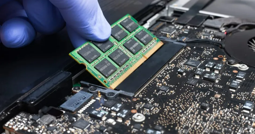
Multilayer PCB Applications
Multilayer PCBs can be found in a wide variety of industries and applications due to their ability to meet different standards and because they have many advantages over electronic devices. Here are some common applications of multilayer PCBs:
- Consumer Electronics
- Among others, smartphones, tablets, laptops, and wearables use MLPCBs for their small dimensions, high component density, and advanced processors.
- Telecommunications
- Multilayer boards of network equipment such as routers, switches, and communication systems are useful for their high-speed signal processing, reliable connections, and compact design.
- Computing and Data Storage
- Multilayer PCBs are used in servers, data storage equipment and their data centers because they consume low power, carry high-speed signals and maintain tight buildup between various components.
- Automotive Electronics
- Multilayer PCBs are the go-to solutions for automotive control units, infotainment systems and advanced driver assistance systems (ADAS) because of their ability to withstand rugged conditions, high temperatures and environmental disruptions.
- Industrial Equipment
- Industrial control systems, automation machinery, and manufacturing equipment apply multi-layered PCBs for their durability, accuracy, and resilience to withstand severe operating conditions.
- Medical Devices
- Medical imaging equipment, patient monitoring systems, and diagnostic devices use multilayer PCBs for their superior reliability, signal accuracy and compliance with safety standards, which far exceed the requirements of regulatory agencies.
- Aerospace and Defense
- Multilayer PCBs are employed in air avionics systems, satellites, radar systems, and military electronics for their parameters like lightweight mechanism, high performance capabilities, and the ability to resist vibration and shocks.
- LED Lighting
- PCB assemblies are widely used in LED displays, lighting fixtures, and signage due to their abilities to manage the power distribution system, thermal management, and accurate control of LED arrays.
- Renewable Energy
- Multilayered PCBs are used in solar inverters, wind turbines, and battery management systems to achieve high conversion, system efficiency, reliability, and power electronics component integration.
- IoT and Embedded Systems
- (The run of devices, embedded systems and sensor networks on MLPCBs, including a small form factor, low power consumption and connectivity options, is enabled with IoT devices and sensor networks.)
These multilayer PCB types are demonstrated in practical applications, demonstrating their importance across different industries. Deaths bodies’ flexibility, trustworthiness and performance make them critical elements for the creation of modern electronic components, devices and systems.
Choosing the Right Manufacturer for Multilayer PCBs
Selecting the optimal PCB manufacturers for multilayer PCBs can make the difference between product excellence and poor performance. Thus, this decision is of paramount importance for electronic products. Here are some factors to consider when selecting a manufacturer for multilayer PCBs:
- Experience and Reputation
- Look for PCB manufacturers with a proven track record as well as vast experience with delivering products of these kind. Ensure that you check reviews, testimonials, certificates, and possibly any awards for the company’s image and credibility.
- Quality Standards
- Make sure that the manufacturer meets up the strict quality standards and certifications, for example, ISO 9001, IPC-A-600, and UL certification. Reliable PCBs can be achieved throughout the manufacturing processes only when quality is entrenched through the processes.
- Advanced Technology and Equipment
- Select a manufacturer that has the latest state-of-the-art facilities, advanced manufacturing technology, and high-precision parts and equipment. This allows for the precision placement and routing of interconnection traces down to the millimeter level, as well as inspection equipped with automated optical imaging (AOI) to guarantee top-tier accuracy and detail.
- Design and Engineering Support
- Try to find companies that provide full-service consulting, which can help you in the multilayer PCB manufacturing process. It includes a review of the design quality, DFM analysis, and prototyping services to make the process more feasible and functional.
- Material Selection and Sourcing
- Assure that the manufacturer uses first-grade materials which came from trustworthy suppliers. The diffusion brazing furnace suppliers should provide a wide profile of substrate material, copper thickness gaps and surface finish alternatives to suit your particular needs and preferences.
- Customization and Flexibility
- Decide on a manufacturer that offers flexibility in terms of order quantities, lead times and customized options. This should be done in a way to allow them to take into account your individual specifications, such as board size, number of layers, and other unique features, to follow what your project requires.
- Cost and Pricing
- Besides the cost, the quality and reliability of the product should be emphasized rather than the price alone. Study the prices of more than one manufacturer, but also take into account other factors like manufacturing capacity, material quality, and technical advice while determining its true worth.
- Customer Support and Communication
- Find companies that listen to you and communicate with you all through the manufacturing process in a clear manner. They should contact you if there is something that they do not understand in order to enable you to make arrangements, and they need to keep you informed about your order from production to delivery.
It is very important to consider these factors as well as do research so that you select a manufacturer that makes multilayer PCBs that meet your quality, performance, and budgetary needs.
Conclusion
Multilayer PCB advantages are characterized by numerous important features, such as increased device density, improved transmission quality and power distribution and better thermal management. Their adaptability to different application fields, including consumer electronics, telecommunications, automobiles, aerospace engineering, and medical gadgets, is one of the factors that distinguishes them from all other metals. The identification of multilayer PCBs implies considering such factors as experience, reputation, quality standards, technology, design support, material sourcing, and customization options. Other factors you should look at include cost and customer support. Through the selection of the right manufacturer and by harnessing the power and ground layers of factors like these multilayer PCBs, we will pave the way to ensuring the quality, reliability, and performance of the electronic products, which in turn will lead businesses to achieve success in competitive markets.