Immerse yourself in the intricate principles of PCB design by reading through our detailed guide optimized for building top-notch 4-layer stackups. Study the latest isolation techniques, current handling and VHF/UHF signal distribution solutions. Understand how to use latest new materials and advanced technologies to improve reliability and efficiency. Whether you have been in PCB design business for long time or you are starting with this PCB design school, the information and skills in this guide will help you create designs that meet the toughest performance specifications.
What is a 4-layer PCB stackup?
4-layer PCB (printed circuit boards) is a kind of circuit board that made up of four different conductive layers interspersed with insulating layers. This circuit embedding process is performed in multiple layers and the stacking of all these different layers together results in a finished circuit board. In the 4-layer PCB, the conductive layers are nestled in a blob-like form and divided by insulating materials. It means that the chip-level PCB structure is more complicated and has a smaller millage than of the single- or double-layer ones. The additional layers offering more routes for the traces to follow can play a vital role, as this facilitates the reduction of signal interference, better distribution of power delivery and minimization of noise for which the overall performance is much better.
4-layer PCBs are seen in many types of electronics equipments, in particular those with complex circuitry like computers, mobile phones, and networks which need special circuits. They present the right complexity level versus cost while delivering generally good performances, which can be an advantage for many applications.
Key components of a PCB Stack-Up
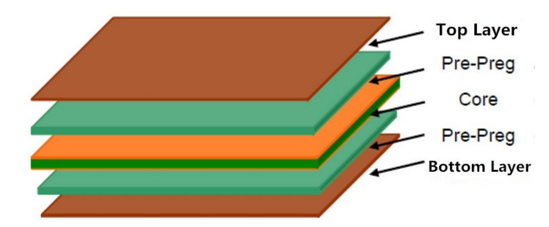
- Copper Layers: These are the conductive layers where we form traces, pads, and vias that are the basis of the whole connectivity between components on the PCB.
- Insulating Layers (Dielectric Material): These layers are the ones which electromagnetically isolate the copper layers and provide electricity into them. The types of dielectrics are chosen, focusing on factors such as dielectric constant, dielectric thickness, and mechanical properties.
- Prepreg Layers: Prepregs (pre-impregnated) layers are a semidry type of dielectric materials that is partially cured and is used to bond the copper layers together. The prepreg layers will be located between the copper layers and will become active when the PCB manufacturing process exhausts to render a resilient bond.
- Core Layers: At its outermost, the core layer dielectric material is in the form of solid sheets, with copper foil being double-sided. These inner layers hold the electrical components together. They make up the heaviest part of the printed circuit board.
- Solder Mask Layers: Over and under solder mask layers are used to shield outside the copper traces as well as from environmental pollution and solder during production time.
The precise arrangement and better power distribution of the components (i.e., layer placement in stackups) can be affected by design parameters such as signal integrity, power distribution, thermal management, and fabrication. One of the techniques is to place different stackup configurations in different electrical performances and EMI, besides seeking to satisfy mechanical requirements of varied applications.
4-Layer PCB Stackup
These are the four-layer PCB stackups:
Top Layer (Signal)
This topmost layer is the signal layer, which consists of signal traces, component pads and vias for routing the electrical signals to the necessary components. Data is borne on the trace signals and also carries the control signals and other electrical signals throughout the outer layers of a circuit.
Inner Layers (Ground and Power Planes)
The merged inner layer now merges both the functions of the ground plane as well as the power plane. It is a very basic and permanent layer whose main function is to serve as ground-route power plane for signal return paths and power distribution to components.
- Inner Layer 1 (Ground Plane): The first inner plane is most of the times continuing over the whole ground. This number of layers provides a reference for the return path of signals and it is the way it provides a low impedance path for current flow, reducing electromagnetic interference (EMI). The low-cost way to deal with noise immunity and signal integrity is by using a ground plane.
- Inner Layer 2 (Power Plane): The second inner layer is generally equipped with power plane, which is a stability voltage provider for components on the PCB. It distributes power around the components and helps with regulation of the voltage so the it can be at the same level at every point in the circuit. This part also helps reduce voltage rot and hikes in the power distribution system.
Bottom Layer (Signal Layers)
Similar to the upper layer, this outer layer contains the signal tracks, component pads, and vias for routing electrical signals. It achieves the completion of the looping of signals that could well have been beyond the hallmark layers and offers additional circuit routing flexibility.
This 4-layer stackup offers several advantages, including:
- Improved Signal Integrity: The grounding lines and power planes enable the minimization of signal distortion and crosstalk, as well as reduction of noise, resulting in a better signal.
- Enhanced EMI Shielding: More layers with ground planes inside are shielding, and thus they do not let electromagnetic radiation out and do not influence to outside interference.
- Simplified Routing: Featuring many layers for routing ultimately results in enclosed and dense path application, which is great for a better path management stage.
- Better Thermal Management: Planes of power lead paths out for generated heat helped with thermal management as deregulated the overheating problem.
This slanted stack configuration, which directs each signal to proceed in the shortest path, is designed to balance the best signal integrity between noise reliability, suitability for manufacture, and cost in order to make it appropriate for a variety of electronic applications. Nevertheless, there are some stackup configuration spreads and options are based on the function of the PCB circuit board and its intended role (the application).
4-Layer PCB Stack-Up Layout Design Considerations
The design of a 4-layer PCB stackup has some crucial factors that need to be carefully considered to achieve good performance, signal integrity, and manufacturability. Here are key design considerations for a 4-layer PCB stackup:
- Layer Configuration:
- Decide on the arrangement of layers. Usually, a 4-vert stack-up comprises two signal layers at the end and two plane layers in the middle (VCC and Power).
- Determine the purpose of each layer. Signal layers are key carriers and components, while internal layers such as power and ground are the traces for return path signals and power.
- Signal Integrity:
- Minimize signal distortion and interference: Keep all fast signal lines short and direct; never cross fast signal lines.
- Control impedance: Form design with proper widths and spacing to obtain a characteristic impedance in accordance with high-speed signals, particularly.
- Use differential pairs: transfer signals closely together to have proper signal integrity but maintain disconnection between them to reduce common-mode noise.
- Power Distribution:
- Ensure stable power supply: Use only one layer of internal wiring, which will provide power for other components.
- Place decoupling capacitors: Incorporate decoupling capacitors in the right-places between the power and ground planes, close to the power pins of ICs, in order to minimize noises and get stable voltage levels.
- Minimize voltage drops: Plot the power plane design as those paths have low impedance and drop almost no voltage; moreover, those having high current requirements may cause voltage drops.
- Grounding:
- Create a solid ground plane: Incorporate low impedance pathways that define the other internal layer as continuous ground plane to eliminate noise and improve signal integrity
- Connect components to ground: Directly connect to ground plane using vias, which is a good path terminating, thus minimizing ground loops and lowering the noise.
- Separate analog and digital grounds: If this approach must be used, divide sensitive analog ground from digital grounds. Such a procedure is necessary to keep digital ground, which is noisy, away from the analog ground.
- Thermal Management:
- Distribute heat evenly: The thermal vias are trying to dissipate the heat from the components through the ground plane or the heat sink, which is outside.
- Avoid hotspots: Provide power and ground planes uniformly to avoid developing heat spots and thermal problems, eliminating the growth of hotspots, especially in high-power applications.
- Manufacturability:
- Consult with the PCB manufacturer: Guarantee that the selected stack-up variation is in sync with the manual applying them.
- Consider material properties: choose the proper substrate material for the PCB and ensure adequate copper thickness to sustain a high current load and keep heat dissipation near the desired level or under control.
- Verify layer alignment: Decide on the stack-up configuration that provides good layer-to-layer registration accuracy throughout manufacturing; tight tolerances shall be applied.
- EMC/EMI Considerations:
- Minimize electromagnetic interference (EMI): Lay out the PCB stackup that will not add more susceptibility to external noise and reduce radiation.
- Use shielding: An illustration may be the inclusion of barriers, shields, or shielding layers around vulnerable components or regions so that these can be protected from electromagnetic emissions that stem from the basic system, and this one can also be protected from susceptibility.
Through proper deliberation of the abovementioned design features, you can develop a PCB layout stack up that is robust, reliable, and efficient and also suits the application requirements and manufacturability.
Common Design Tools used for 4-Layer PCB Stack Ups
Different design tools are applied wide-rangingly to creating 4-layer PCB stack-ups with high frequencies and attributes favorable for design, simulation, and analysis. The number of tools to be employed in this campaign largely depends on factors including budget, preferred features, and comfort being acquainted with them.
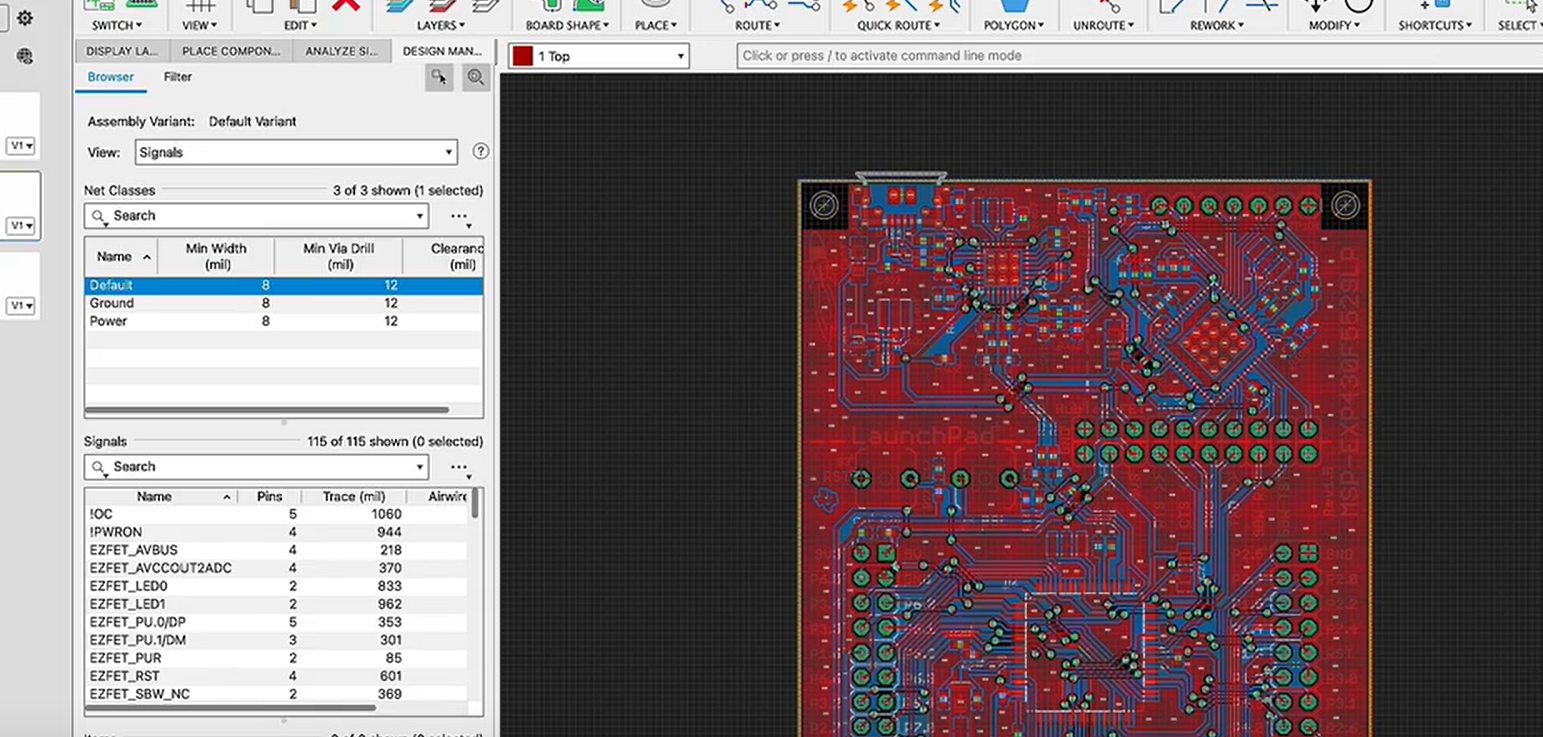
Altium Designer
Altium Designer is one of the most popular PCB design applications and has extensive functions to make circuit diagrams, board layouts, and view 3D models. It have multilayer circuit boards stack-up tools for arrangement and simulation, as well as harness and impedance analyzer and a signal integrity tool.
Cadence Allegro
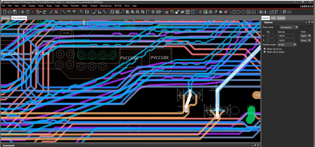
Cadence Allegro, yet another efficient product in the PCB design tools PG/PCB suite, stands out for its multi-functional specifications in high-speed and high-temperature mixed-signal designs. It has utilities for stratus bed planning, routing, simulation and manufacturing preparation.
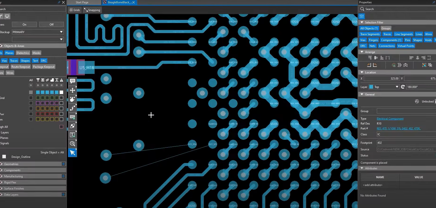
Mentor Graphics PADS
PADS was developed by Mentor Graphics as software for creating new PCBs and accomplishing PCB layout. It provides simulation tools for making and modifying a multi-layered structure, such as for instance, the characterization of impedance as well as thermal analysis.
KiCad
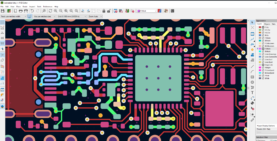
KiCad is”free software used for creating PCB (Printed Circuit Board) designs by hobbyists and professionals. The suite of tools that comprise it consist schematic capture, PCB layout, and 3D visualization, and it is an open model that can be used for simulations and multi-layer stack-up creation.
OrCAD PCB Designer
OrCAD PCB Designer is one of the OrCAD package of tools that allows for segmentation, schematic capture, PCB layout, and simulation processes. It is the construct that encompasses operations on features such as multi-layer stack-up generation, impedance control and analysis of signal integrity.
Eagle PCB
Eagle PCB is a common PCB design tools which is very easy to use and includes a large collection of Components. The benefit of having multiple-layer simulation capabilities might not be as advanced as some other tools, but it has what needed to stack the top and bottom layers and extra for basic simulation.
HyperLynx
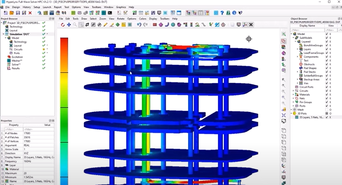
Mentor Graphics presents HyperLynx, a software which is used for modeling and simulation of PCBs and provides features of signal integrity, power integrity and electromagnetic interference analysis. It is not a PCB layout tool but can be used in tandem with other layout tools for verification and optimization component placement of laminations, which are the insulator layers that embedded circuit can be placed on.
4-Layer Stack Up Design Considerations for High-Speed Signals
A good 4-layer PCB stack-up for high-rate digital signals must be premised on several considerations so as to allow signal integrity, impedance control, and electromagnetic compatibility.
Here’s a breakdown of key design considerations:
- Impedance Control: Implement a technique to take care of the high-speed traces that have controlled impedance by using the geometry of microstrip or strip line respectively, and also by carefully working out the widths and distances between these traces so as to achieve the desired characteristic impedance.
- Layer Arrangement: Regarding layer routing, place signals next to solid reference planes, thus maintaining the uniform impedance level and symmetrically array those in order to avoid unequal paths in terms of signal amplitude and switching delays around the entire board.
- Ground Plane Design: Through With the continuous ground planes in place, stable signal returns will become available. The high-speed signals must not be split. The impedance to the ground must be minimized using through-hole stitching.
- Power Distribution: Deploy focuses power planes for stable supply, introduces bypass capacitors to prevent leakage current, considers route length, and reduces inductance and resistance in a power trace design.
- Signal Routing: Count on indirect ways of bringing high-speed signals with short tracks to minimize signal delay times, ensure gaps between paths to decrease crosstalk impacts, and use differential signals for critical signals to increase noise immunity.
- Symmetry and Symmetrical Routing: Strictly maintain the stack-up symmetry and make the routing procedure mirror-matched to get the same impedance and balanced signal through the path in all layers.
- Via Placement and Design: Carefully place the openings to reduce the signal mismatch and use stitching for the interconnection of different signal layers, which guarantees the signal integrity and reduces the variabilities of the impedance.
- Ground Plane Splitting: Break the ground plane electro-servally by applying the grounding method, which will help to keep the signal unbroken and uncross-us.
- EMI Shielding: Implement the shaping techniques like the ground planes and the routing so as to decrease cross talk among the wires and to regulate the impedance. This will thus guarantee error-free transmission.
- Thermal Management: Let’s pay attention to the relationship between heat and the high speeds of electronic components and design for good heat dissipation to help prevent problems related to heat that could change the signal performance.
- Manufacturability and Cost: Extend designing by the PCB manufacture-ability and minimize the disparities between the design requirements and costs so as to achieve good performance and affordability.
Conclusion
To summarize, designing a 4-layer PCB stack-up takes into account signaling layer integrity, impedance control, and manufacturability considerations. Through the placement of signal layers that airbrush the ground plane with the power planes, the impedance control of all the signals and traces is routed in a symmetrical pattern, and the signal will have the right performance and reliability. The designer can then use the 3D design tools for stack-up planning, computer simulation, and analysis, among others, to make sure that the design is efficient for high-speed demands as well as manage the design cost and manufacturability. Proper attention to detail and compliance with best practices will be apt to provide the highest-performing and most reliable 4-layer PCB stack-up configuration that can be used in consumer electronics’ applications as well as spacecraft systems.