Learn how PCBs are manufactured in this easy-to-follow tutorial for a beginner. Take a class on schematic design, material selection, layer stacking, drilling, the plating process, solder mask application, surface finishing, testing, and many more topics. Explore the realm of actual PCB fabrication and learn the secrets behind the production of excellent circuit boards that will give your electronic projects the life they deserve.
What is a Printed Circuit Board (PCB)?
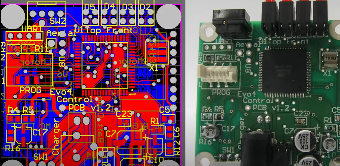
The Printed Circuit Board (PCB) is a vital one in the era of modern electronics and follows this way. It is a non-magnetic flat board consisting of a non-conducting material (good choices include fiberglass or composite epoxy resin) with metallic conduction pathways etched or “printed” on it. These paths, which are usually tinned in copper, connect different chips planted upon the board and enable them to interact with each other.
PCB offers an ideal place for mechanical fixing and mounting critical components such as resistors, capacitors, integrated circuits, and connectors, which are basically the backbone of electronic circuits. Streamlining is the production process term which results in elimination of unnecessary wiring and soldering of components everywhere, that in effect makes devices more reliable, compact, and cheaper for consumers.
What are the Parts of a Printed circuit board?
The the printed circuit board assembly (PCB) has different constituent parts, all of which have a specific role that gives the PCB functionality and makes its construction possible.
Substrate/Base Material
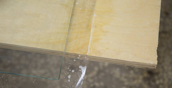
The substrate of the PCB is typically made of fiberglass-reinforced epoxy laminate and is the base layer upon which the rest of the PCB is constructed.
Copper Layer
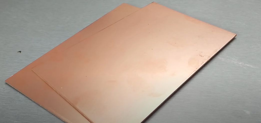
About uniformly thin layers of the copper sheet are laminated on the substrate. Copper connected these layers, and this mass of copper is what is known as traces that carry electrical signals between the components.
Pads
These are traces of the copper foil layer, which are the points where components are joined to the board through the soldering process. Pads are the places that carry the pins of the components and the traces on the PCB.
Traces
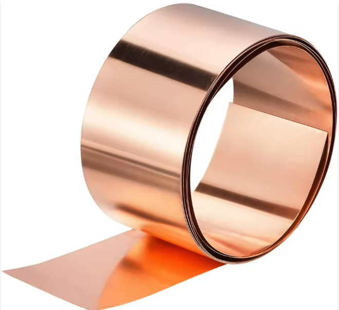
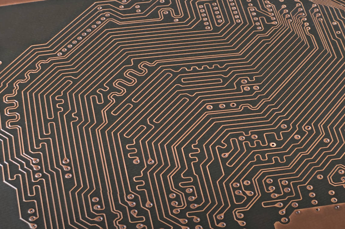
These are the structures on the PCB that are responsible for conducting the current and connecting other components. As a rule, traces are manufactured with copper and laid on the PCB surface.
Vias
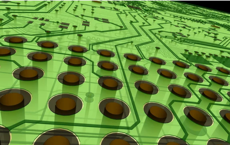
Via are small plated functional holes drilled through the PCB substrate. Conductors allow electrical bonds to form between different layers of the board, like the inner and outer layers.
Solder Mask
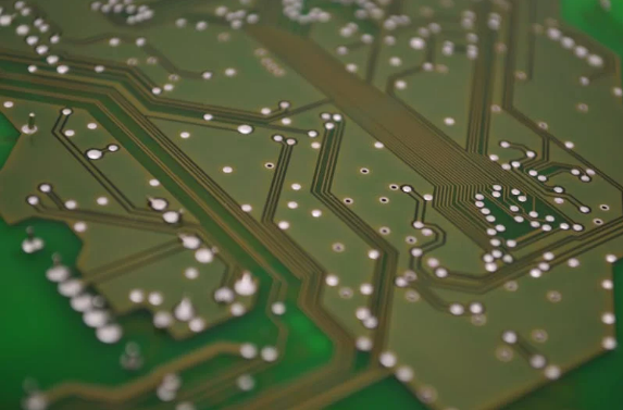
On top of the copper layer, which is covered with a polymer, only the pads are exposed. The solder mask acts as a UV protective layer to prevent traces from oxidation; in addition, it prevents accidental electrical connections during soldering.
Silkscreen
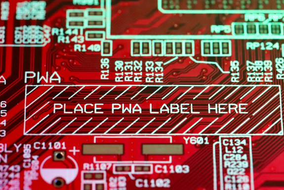
This is what we call the topmost layer of the printed circuit board, where the elements that are not components, such as component outlines, reference designators, logos, and other information, are printed. The information will aid in the process of component placement and PCB assembly.
Components
They are the electronic components attached to the PCB that can be resistors, capacitors, integrated circuits (ICs), connectors and so on. Parts are then placed onto pads on the the PCB surface or inserted into holes and soldered.
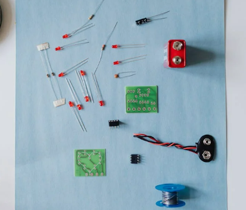
Mounting Holes
These are holes machined on the PCB board that are used for mechanically fastening it to its casing or assembling the board onto other components.
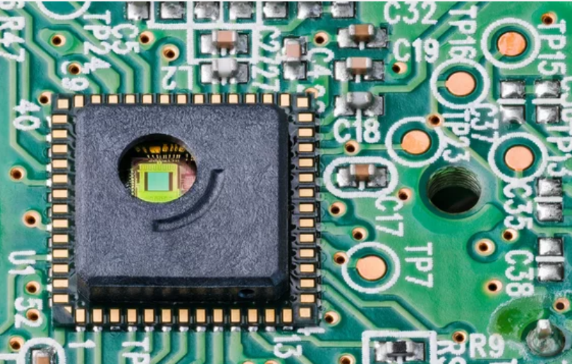
PCB Fabrication Process Design
The PCB fabrication process of circuit board development begins with designing and preparing the layout and design files that will be used for the manufacturing of the printed circuit board (PCB). Here’s a detailed overview of the PCB fabrication design process:
- Schematic Design: It usually begins by creating a schematic diagram of the circuit using specialized programs like Altium Designer, Eagle, or KiCad. In the connection design stage, the electrical components are placed on a substrate and nets to show actual electrical connections are used for interconnecting these components.
- Component Selection: Once the schematic is finalized, designers choose components for the circuit based on functionality, technical requirements and availability. There will be a selection of parts which should fit the given design constraints, like size, power consumption, price, etc.
- Footprint Creation: For every component selected, designers draft drawings that depict the size of footprints. Footprint are the ones which define the physical layout and dimensions of every component’s package pins and mounting holes on the printed circuit board. They can serve as the guiding object for component positioning and soldering during fabrication operations.
- PCB Layout: Schema will be a basic tool that designers will use to create the PCB design process by positioning the components and designing the traces between them. The next step in the process is to look into the line width, power distribution, thermal control, and power integrity. Designers target the minimum trace length by avoiding timeliness reducing signal crosstalk, and designing those for manufacturability.
- Trace Routing: Via serves as the way or medium to make the component in the loop gets currently connected in an electrical path based on the circuit design. Designers may be utilizing different routing styles, for example, orthogonal routing, 45-degree routing, and differential pair routing, through which signal integrity problems can be optimized and better EMI/EMC performance could be attained. The high speed leads to self-imposed impedance routing, which maintains impulse signal integrity.
- Layer Stackup Design: The stack-up will be decided based on the complexity of a circuit to be produced and design requirements that the PCB designer has to execute. The layer stackup determines the signal impedance by the number and sequence of the transmission copper traces, dielectric layers, and internal signal references. Layers stackout has to be applied in appropriate manner for the purpose of meeting the required electrical characteristics and signal integrity.
- Design Rule Check (DRC): After the layout has been finished, designers will then proceed to a design rule check that will verify manufacturing constraints and design rules compliance. DRC checks values like trace width, spacing, clearance, and hole size, which are critical for the intended fabrication, by an automatic file by the machine.
- Gerber File Generation: After completing DRC and the design being looked into, designers compile Gerber files and other manufacturing files that will be used in PCB fabrication. Gerber usually comprises the amount of copper in the layers, solder mask, silk screen and drill details required for PCB manufacturing process.
- Design Validation: Operations such as EDA (electrical design automation) are used by designers before sending the design files for fabrication. These could include signal integrity analysis, thermal analysis, and 3D modeling. A validation process is very useful as it enables us to detect and correct errors at early stage of the design.
- Documentation: Designers put together documentation, including fabrication drawings, BOMs, fabrication notes, and assembly notes, for manufacturing partners to aid them with design file production and assembly.
- Prototype Fabrication: When the design documents are completed, the PCB is fabricated and then prototypes or small batches of PCBs for testing and validation are made. Developers might make changes on the initial design after achieving the results of testing, although a prototype is not an actual product itself.
PCB Manufacturing Process
The PCB fabrication process is multi-stage and encompasses multiple steps which are intended to transform a design file for printed circuit boards (PCBs) into a physical product.
1. Design Preparation
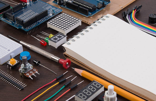
Engineers generate the circuit schematic diagram and then turn the circuit layout into PCB design using specially equipped software. This option involves both the placement of components and the patterning of cables infrastructure.
2. File Generation
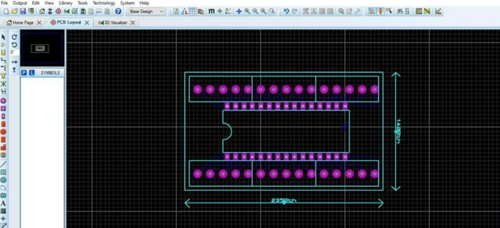
The Gerber files are produced with a production-only PCB layout file. The Gerber files contain copper layers, solder mask, and silkscreen, which also have information about characteristics and properties . In addition, drill tables are created, which the board manufacturers use to drill the necessary holes into inner layers unwanted copper part of the PCB.
3. Material Selection
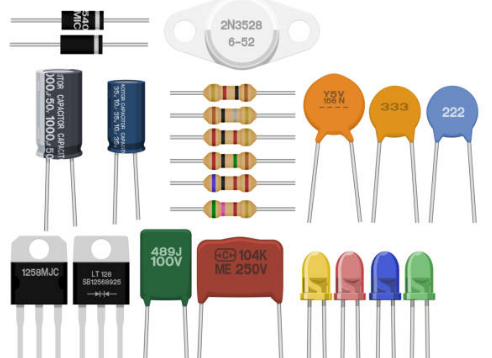
The main material for over lays of the inner and outer layer imaging of the PCB, that may be FR4 fiberglass, is selected based on the required electrical and mechanical property. Thin copper foil is coupled to the base to conduct the signal.
4. Preparation
The substrate is made clean to avoid any molecules which may cause bond failure. It is chunked into PCB board sizes, and the product is then cut into individual board sizes to allow the PCB design process.
5. Layer Stacking

The substrate and outermost copper foil layers are stacked by a machine for the patterned alignment of unwanted copper foil, which completely satisfied the needs of the design. This prepreg sandwich system comprises laminates of glass fiber impregnated with epoxy resin, and between these layers is the copper that acts as the conductor.
6. Drilling

Beyond the outer and inner layers of stacking, automated drilling machines accomplish the drilling of holes for through-hole components and vias into the stacked panel for later UV passthrough. The fact that the holes are drilled is one of the things that are made to make the tooling registered and aligned.
7. Through-hole Plating
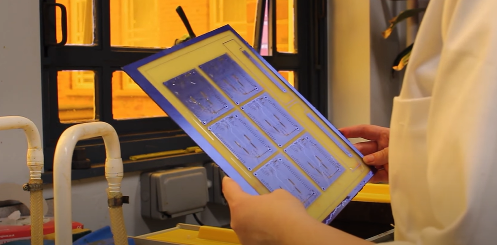
The holes are drilled where the surface of the material is made of conductive copper traces so that plating can be performed. Copper electroplating resembles and is employed inside the holes; due to this, the current paths among inner and outer layers of multiple copper layers are solely electroplated.
8. Copper Etching
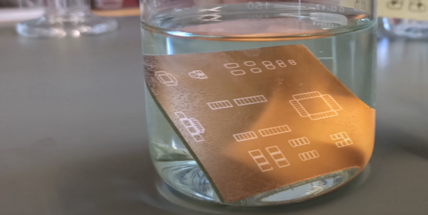
The photoresist in an ultraviolet (UV) light-exposed layer is spread over the copper surfaces of the circuit board. Through the photomask, UV light is used to expose them. After this, chemicals are used as part of the process to selectively expose exposed copper to ultraviolet light, leaving the traces unwanted copper you want to keep behind it.
9. Solder Mask Application
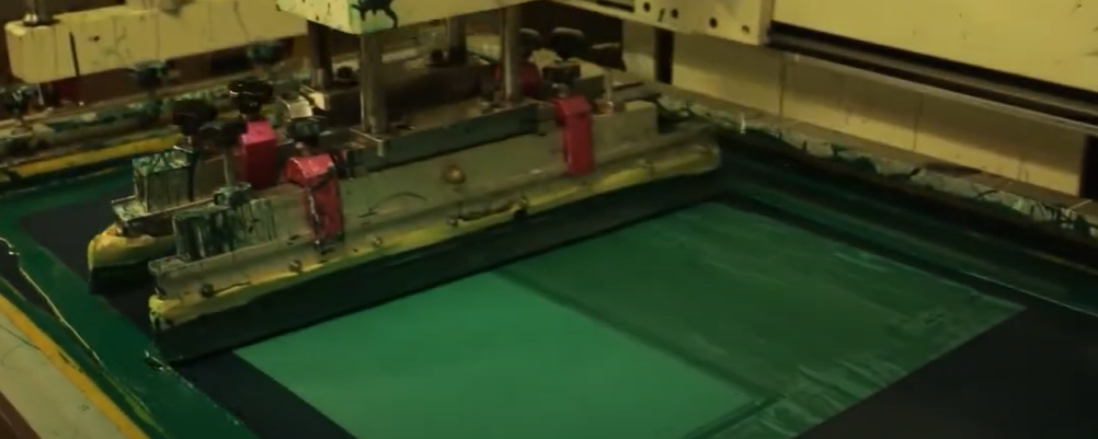
The board is covered with solder mask ink ink that can be applied as a thin layer and only on those areas where components are not supposed to be soldered with solder. After the thin solder mask layer is placed, the corresponding ink is cured to enable inner layers of it to withstand the soldering heat and last longer.
10. Surface Finish Application
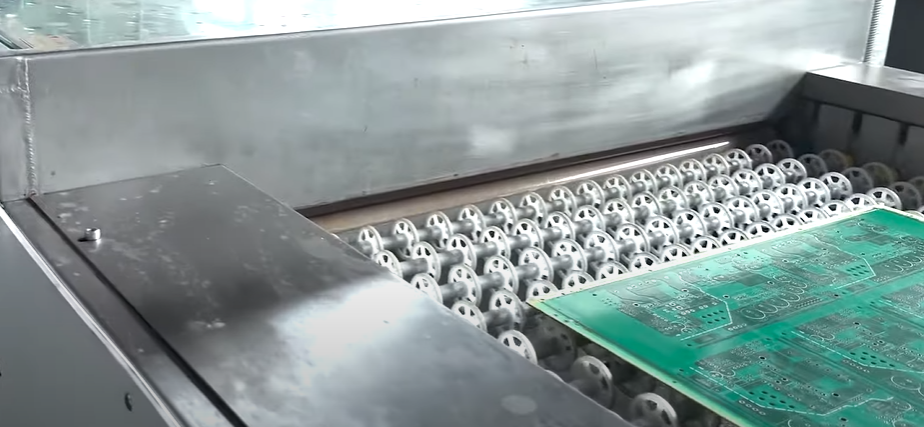
Exposed excess copper on surfaces to be cleaned and a coating could be applied for a finish process. The most used surface finishes include HASL (Hot Air Solder Level), ENIG (Electroless Nickel Immersion Gold) and OSP (Organic Surface Protectant), which place solderability and excess copper oxidation protection at the center of their function.
11. Silkscreen Printing
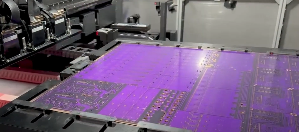
All the necessary component schematics, labels, and other symbols are printed using a silkscreen printing procedure onto the boards’ print surface. The ink is cured so as to enhance the product life and enable the component to be set up or situated properly.
12. Testing and Inspection
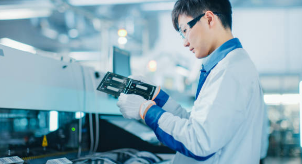
PCBs gets physical and electrical test is done to make sure that their connectivity, electrical shorts, and opens are tes It is also vital to do visual inspection where I will be focused on defects like solder bridges, missing parts, and misalignment.
13. Finalization
Separating the sound-opaque boards from the final panel with the aid of routing or scoring is possible. At the time of final inspection, all the PCBs will be checked and confirmed that they are in compliance with set quality standards before they are decided to be packed and get prepared for shipment.
Printed Circuit Board Manufacturing Basic Requirements
The basic requirements for PCB manufacturing process include:
- Design Files: It’s very important to have good and clear design files in appropriate formats (for instance as Gerber or Excellon) for manufacturing. File contents should be composed of cooper layers, solder farmasak mask, silkscreen and drill patterns and other additional information such should be indicated.
- Material Selection: There could never be a superior performance and reliable PCBs without making the proper choice of high-quality materials. Such selection would involve FR-4 fiberglass substrate, type of copper foil, solder mask type, and printing surface finish.
- Fabrication Equipment: Computer boards involve various machineries and equipment category which involve CNC machines for drilling and routing, exposure unit for imaging photoresist, plating of through-hole tank, and reflow ovens for soldering surface components.
- Skilled Workforce: A trained and experienced manpower or workforce is vital as they will be the ones to operate the manufacturing machinery, understand the design files, resolve issues as well as guarantee product excellence.
- Quality Control Procedures: A rigorous quality assurance system functioning narrow-minded to resolve condition of defect occurring during manufacturing is very important. It is basically being conducted through the visual inspection, electrical testing, as well as the observance of the industry standards and parameters.
- Environmental Considerations: PCB production should be guided by environmental precautions and best practices, worldwide, with a view to reducing environmental harm when possible One of its aims is reducing, reuse, and proper disposal of the wastes as well as effective energy use and conservation of water.
- Testing and Inspection Equipment: Testing and inspection tools, including automated optical inspection (AOI), X-ray inspection equipment, and electrical tester, should be used before the final shipment for verification of PCB quality and functionality since you want the final product your customers will be happy with.
- Documentation and Traceability: Suitable documentation and traceability systems should be in place to follow the entirety of the manufacturing process, including identifying problems and any deviations or tendencies, as well as maintaining constant product quality whenever it is desired.
- Customer Requirements: It is necessary to have the ability to understand and face customer requirements, including technical provisions, quality requirements, lead times and prices, if PCB manufacturing process is to be considered successful.
- Continuous Improvement: Adopting a culture of constant improvement permits continuous improvement of activities, equipment, and processes, which leads to end points of higher efficiency, better quality and satisfied customer.
How do you implement an effective PCB manufacturing process?
To build PCBs, one should create a circuit board manufacturing process in which all factors are carefully considered and all industry quality factors are respected. Here are some key steps to implement an effective PCB manufacturing process:
- Define manufacturing goals and requirements:
- Be specific and clear. Layout the plan for the PCB manufacturing production system. The system should contain features such as quality, volume, timeframe, and costs as well.
- Select suitable equipment and technology:
- Decide on the necessary equipment and technology that are suitable for the type of manufacturing you want to undertake. The technology to be used for the printing circuit boards and testing and inspection systems may all be part of your project.
- When defining good equipment with those parameters, keep in mind production capacity, product complexity, and your budget.
- Establish Quality Control Procedures:
- Implement rigorous quality control norms to guarantee security, consistency, and an acceptable standard of manufacturing.
- Verify the specification compliance and quality level at various production phases by setting checkpoints to detect and eliminate any defects and deviations from specifications among the samples guided afterward.
- Train Personnel:
- Develop and put in place skill training and continuous education for the staff, operators, engineers, technicians, and quality control people in the actual ramping up of the PCB manufacturing process.
- Preparing the staff by teaching them how to handle the equipment as per the safety rules and high standards. Staff will also be updated on the current best practices for their jobs.
- Optimize Workflow and Process Efficiency:
- Study the process lines in terms of actions and charging pipelines for the elimination of downstream lags, acceleration of cycle time, and finally efficiency.
- Lean manufacturing aspects like just-in-time inventory management and continuous process improvement programs will be put in place to achieve positive returns in areas such as key resource utilization and waste minimization.
- Implement robust supply chain management.
- Maintain good relationships with usual direct suppliers and vendors on time delivery; no raw materials, components, or equipment will be out of stock.
- Scheduling is important in production and cuts the risk by keeping the product available during the issuing process.
- Utilize Advanced Manufacturing Technologies:
- Keep abreast of the treatment technique, latest PCB manufacturing technology, materials, and methods to set off the product’s progress, performance, and cost effectiveness.
- Look at different options for how automation can be done, too, as well as robotization, additive manufacturing, and digitalization solutions, all of which should be guided towards raising productivity and adaptability.
- Monitor and analyze performance metrics:
- The key success factor lies in the effort of developing a set of KPIs (Key Performance Indicators) that can be utilized to examine and evaluate the execution of the PCB (Printed Circuit Board) manufacturing process. Criteria comprise the number of defects, the yield rates, cycle times, and customer satisfaction, which can be used as indicators rather than the means to judge the program.
- Apply the integrated techniques that employ data analytics and real-time monitoring to identify effective trends, the root causes of issues, and areas with potential for process optimization.
- Maintain Compliance with Industry Standards and Regulations:
- Pay attention to ensuring that your company conforms to the established standards and directives, such as IPC standards, RoHS directives, and ISO quality management systems.
- Incorporating checking, modification, and updates to the process and procedure can create a harmonious environment for policies and processes that need to be in compliance all of the time.
- Continuous Improvement and Innovation:
- Develop a continuous progress and innovation drive within the organization where the participation of all employees as co-developers of the process is highly encouraged to achieve the highest quality of printed circuit boards.
- Track and manage the facilities and equipment, the procedures, and the techniques of production to be able to identify their best sides, which can be used in your venture.
Why is it important to understand the PCB fabrication process?
Recognizing the PCB assembly process is fundamental to the production of high-quality, cost-efficient, and cost-effective printed circuit boards. It is helping designers, producers, and industries improve their processes, cut costs, raise quality, and spark renewed competition in the market. Here are some of the reasons:
Design Optimization
Having studied the manufacturing process, designers of PCBs are able to create optimum layouts for manufacturability. Powered by a knowledge of the existing practical framework, I insightfully understand how far is possible to go with design and what needs to be excluded since mistakes in this area would lead to either manufacturing defects or a lengthy process of reworking complex process.
Cost Reduction
Knowledge of how the process works develops ability of design engineers, making them make right and sustainable decisions that can subsequently decrease the manufacturing cost. Through materials efficiency, less waste production, and smoother process optimization, the manufacturers are able to both make savings on expenses and reduce the products’ performance.
Quality Assurance
Knowledge of fabrication process is very influential on the quality management system of manufacturers, which is oriented at achieving the quality of PCBs consistent with the specifications and performance requirements. In this way, manufacturers are able detect the problem areas during the process of development that are likely to lead to poor performance and thus take measures to maintain the requested product quality and consistency.
Lead Time Reduction
The possession of this knowledge makes it highly likely to cut down on fabrication times and lead time. Through effective scheduling and planning of production dates, reduced setups, and facility utilization, the PCB manufacturing process can be hastened to gain access to data in tight deadlines.
Innovation and Problem-Solving
An appreciation for the manufacturing process encourages the development of novel and insightful infographic features on the subject. The insight gained into new materials, technologies, and techniques will enable manufacturers to explore new directions and areas in which they might solve manufacturing issues with innovative solutions, thus driving the process of continuous improvement
Customer Satisfaction
deep understanding of the procedures of the PCB fabrication process makes it possible for PCB manufacturers to produce boards that conform to customer demands. Consistency and reliability, including the shortened lead time and lowered costs, manufacturing companies give to customers will increase their satisfaction level and create loyalty.
Regulatory Compliance
Compliance with the standards of the manufacturing process through knowledge of regulations is essential for environmental aspects. With knowledge of effect of manufacturing processes on product risk, quality and sustainability, manufacturers would therefore meet the legal demand and acquire the industry’s most satisfactory practices.
Environmental Considerations in PCB Manufacturing
green influence of PCB manufacturing is paramount to safeguarding the environment from the manufacturing processes and ensuring sustainability. Here are some key environmental considerations in PCB manufacturing:
- Material Selection:
- Select recyclable and halogen-free processable materials with the minimum level of environmental impact, including lead-free solder or environment-friendly substrates.
- Go for material that can fit into the RoHS standards and the REACH standards in order to maintain a low level of toxic substances in your product.
- Waste Minimization:
- Put into practice the strategies that minimize waste at the manufacturing stage in order to decrease the amount of generated waste.
- Rather than disposing of materials, they can be recycled and reused wherever possible: copper scrap, solder, and substrate ones.
- Properly dispose of hazardous waste in accordance with local legislation to avoid polluting the environment.
- Energy Efficiency:
- Improve the energy efficiency of manufacturing processes by making the information process in various equipment easier, reducing the time spent idling, and implementing energy-saving technologies in the system.
- Refit the existing energy-efficient equipment and machinery by installing the latest technologies to consume less energy and release fewer greenhouse gases.
- Water Conservation:
- Implement water resource conservation measures to stop water usage for manufacturing processes where relevant, for example, by recycling wastewater and using water-efficient equipment.
- Reduce water pollution by generating wastewater treatment systems that ensure that toxic contamination is controlled and release to the environment is minimized.
- Air Quality Management:
- Control the discharge of manufacturing processes into the environment by installing efficient air pollution control systems like scrubbers and filters.
- Establish an air quality monitoring system at the production facility so it will meet all the established requirements and not affect the health and wellbeing of the workers and those living in the community.
- Green Manufacturing Practices:
- Implement environment-focused manufacturing techniques, including lean production and Six Sigma, to minimize losses, enhance resource efficiency, and optimize the output of products.
- Become environmentally conscious throughout the entire supply chain by identifying and cooperating with environmentally responsible suppliers and those who promote eco-friendly manufacturing processes throughout the supply chain.
- Environmental Management Systems:
- Aim to develop EMS that can proactively determine, oversee, and control the environmental implications associated with PCB manufacturing.
- It is essential to provide necessary environmental policies, procedures, and systems of control measures to ensure that we comply with environmental regulations and are able to improve our performance over time.
- Stakeholder Engagement:
- Get involved with the stakeholders, for example, employees, customers, suppliers, and local communities, to better get people’s attention and instruct them on how to practice sustainability.
- Fostering ways of collaboration and cooperation with non-profit organizations, public bodies, and industrial associations would allow us to tackle common environmental challenges and promote effective solutions.
Design for Manufacturing (DFM) Considerations
Design for Manufacturing (DFM) considerations cannot be disregarded anymore as they are very important for printing circuit boards (PCBs), ensuring quality and lowering the costs of production. Here are some key DFM considerations for PCB design:
- Component Placement:
- Design a plan for placing parts to avoid long runs by signals, signal conflict and enhance thermal characteristics. Group components with similar functions together in order to make the routing of communication between them smoother.
- Clearance and Spacing:
- Ensure sufficient clearance between among the components, traces, and copper patterns to avert electrical shorts and guarantee moldability of the product. Adhere to brand identity and the rules of design.
- Trace width and spacing:
- Choose the proper trace widths as well as spacing that satisfies electric carrying capacity, impedance regulation, and transmission integrity necessities. Keep as rich a traced definition as possible to avoid an increase in manufacturing costs or the occurrence of reliability problems.
- Via Placement and Design:
- Minimize via localization and the right routing to eliminate distortions, mismatching impedances, and manufacturing complexity. Apply blind or buried vias for avoiding layers when justified to reduce the PCB layer count and the signal performance.
- Layer Stackup Design:
- Create a plan for the layer stack optimization that chooses between signal integrity, EMC, and manufacturing cost factors to be considered. Improving transition layers and mitigating impedance fluctuations are very important. These will, ultimately, make the performance consistent.
- Solder Mask and Silkscreen:
- Apply a solder mask to insulate conductive copper tracks and prevent shorts during PCB assemblies. Ball marks for test points, fiducial marks, and component recognizers need to be provided with the solder mask layer openings. A silkscreen legend should be clear and located far from the soldering parts and the testing circuit to avoid overlapping during soldering and testing.
- Panelization:
- Layout PCBs on panels with the highest material utilization and the minimum manufacturing cost in mind. Develop panel designs with internal fiducial marks, holes for tools, and breakaways that will make the PCB assembly process and handling easy.
- Component Selection:
- Choose such parts that are quickly and cheaply produced and fit automated assembly processes. Stay away from out-of-date or exotic (not commonly found) components that can result in production stalls or raise costs.
- Thermal Management:
- Implement thermal features like thermal vias, heatsinks, and copper pours that effectively dissipate heat and therefore prevent components from overheating. Make sure there is an adequate separation zone and air flow radian around the heat-producing components.
- Design Verification:
- Conduct comprehensive design verification and validation through the use of simulation tools, DRC, and prototyping methods as early as possible in the design process. It is essential to identify and rectify manufacturing problems beforehand. Partner with electronic printed board manufacturers to achieve the output required by design.
Conclusion
To sum up, PCB manufacturing process is a multifaceted but vitally important one for creating the basis of devices. From design planning to completion, each phase calls for specialized knowledge that must comply with professional and community standards. Material selection, layer stacking, drilling, copper etching , solder mask application and surface finish testing. Of these, layer stacking, copper etching , and surface finish testing are the main stages. Through the sheath of directed planning, meticulousness, and never-ending improvement activities, manufacturers can bring out excellent PCBs which are compatible with design specification, performance requirements, and customer expectations In the face of technology’s evolution and after the implementation of innovations, the PBC board production industry goes ahead and treads on a path of development of more complicated and basic electronic products.
Frequently Asked Questions (FAQs)
- What is a PCB?
- A PCB (Printed Circuit Board) is a platform which is thin and has insulating material on it with conductive pathways (traces) etched or printed on its surface. This component facilitates the link of the airframe structure to hold the mechanical side and provide electrical connections for the electronics in it.
- What is PCB manufacturing?
- PCB manufacturing is the procedure for creating a physical PCB from given design. The production process has several stages, which include material selection, bulk up, drilling, etching, solder barrier application, surface end and testing, and trying so hard.
- What materials are used in PCB manufacturing?
- The most common materials used in the PCB manufacturing process include FR-4 fiberglass as a substrate, copper foil for conductive tracks, insulative solder barrier ink, and various surface finishes (e.g., lead-free gold or SnAgCu over ENIG, HASL, etc.) for soldering and protection.
- What is the difference between single-sided, double-sided, and multi-layer PCBs?
- On a one-sided PCB, traces are on one side, and on the other side, traces are on a double-sided PCB. Capitalizing the multilayer PCBs, with the multiple layers of conductive traces in-between the insulation allowance, gives designers the liberty to realize more complex circuit designs.
- What are the steps involved in PCB manufacturing?
- Primarily, the PCB production process involves stages such as design preparation, choosing a material, multilayer manufacturing, drilling, filling, through-hole plating and cutting copper, solder barrier application, surface finishing, testing, and finalization.
- What is a surface finish in PCB manufacturing?
- Surface Finish comprises a few different kinds of coatings that are applied to the copper surfaces of PCB boards to improve soldering and protect them from oxidation. Some of the most frequently used surface finishes include HASL (Hot Air Solder Leveling), PACB (Electroless Nickel Immersion Gold), and OSP (Organic Solderability Preservatives).
- How long does PCB manufacturing take?
- The production time for PCB manufacturing relates to many variables, among which are the production volume, the level of design complexity and the lead times of the materials and components. This could be a period that would last from a few days up to even a few weeks sometimes
- What is the role of testing in PCB manufacturing?
- Testing provides end-to-end-testing of PCBs and proving its quality and functionality is mandatory. The function of electrical testing is to ensure that there are no shorts, openings, or connectivity. Moreover, this method also verifies that all components are where they are supposed to be, there are no solder bridges, and there is no missing or misaligned component.
- What are the environmental considerations in PCB manufacturing?
- The environmental waste factor during manufacturing PCB requires consideration of materials such as energy efficiency, water conservation, air quality management, green manufacturing practices, environmental management systems, among others, and stakeholders inclusion.
- How can I ensure quality PCB manufacturing?
- To make sure that the process of PCB manufacturing is of high quality, it is necessary to contact well-known manufacturers who observe industry standards, have experienced workers, follow strict quality control procedures and buy equipment, machines and technologies.

