PCBs, which are commonly known as Printed Circuit boards, play a vital role in modern electronics as the foundation for electronic components to work effectively together. In this article, we’ll go into the realm of PCBs, where we’ll examine the anatomy, manufacturing process, types, and applications.
What is a PCB?
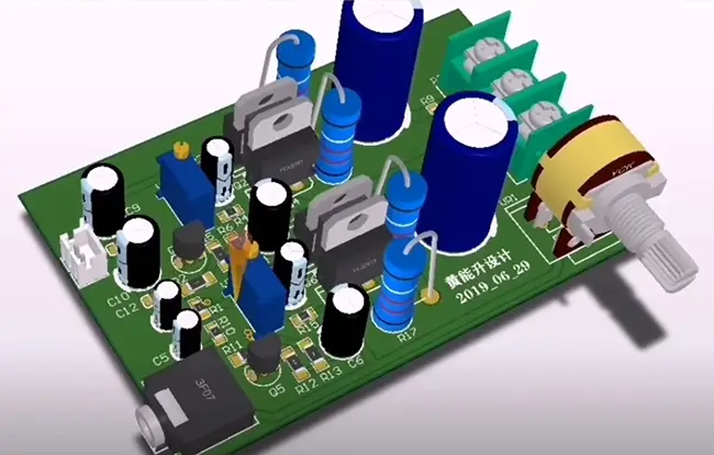
A PCB (Printed Circuit Board), is a flat board commonly made of non-conductive material (usually fiberglass or epoxy) which serves to conduct electricity and help to place and connect the electronic components. These pathways for electricity carry current through the printed board, over which thousands of conductors are etched or printed, typically with copper but possibly also with other materials that conduct electricity like aluminum and tin.
Printed Circuit Board is predominantly utilized in electronics in today`s world as they offer a stable working and joining ground for electronic devices, organizing and assembling them in packages that are small in size compared to the standard ones, thus allowing the functionalities of devices like computers, smartphones and so on.
A printed circuit board is the baseboard for assembling electronic components and their connections to support many types of electronic devices. Printed circuit board layers A PCB can be single-layer, double-layer, or multi-layer.
Anatomy of a Printed Circuit Board (PCB)
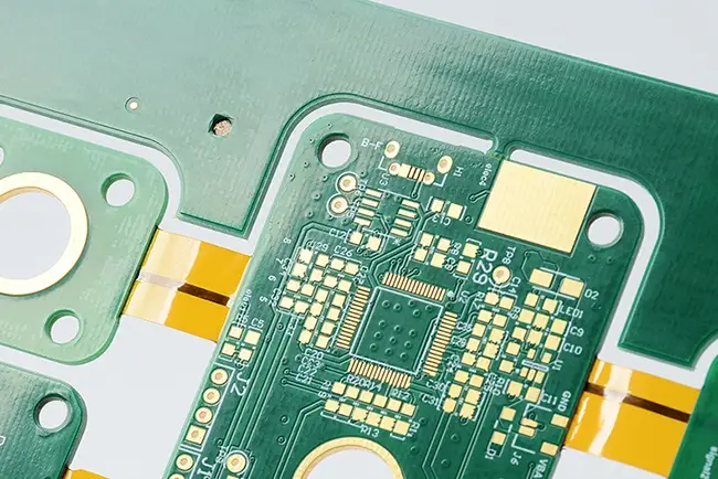
The board is the main body that is usually flat and rigid and is generally made from specialized materials such as glass fibers, epoxy resin, and other similar materials that are not conductive. It is a piece of equipment that consists of lines and pads that connect to each other, forming a certain pattern. They are manufactured from materials that are not conductive but have pads, lines, and etched copper sheets that are electrically connected to different components electronically.
The metal core is most likely made of aluminum, copper traces, or a combination thereof, and this component is deliberately encapsulated between the layers of dielectric material and copper layers . This architecture gives a fixed mechanical frame for the elements of the battery, provides a lower electrical interference, and acts as a barrier preventing the thermal expansion of new parts. They essentially operate like conductive super-highways, where electricity is able to seamlessly pass through the different electronic components soldered.
What are the Layers of PCBs?
Printed Circuit Board is an electronic circuit base that has several layers to help the complex electronics to be compressed and produced. Here are the basic layers of PBC design.
Single-Layer PCBs:
They are the easiest types of circuit boards, comprising a single layer of substrate material, mainly fiberglass or resin. On one layer, components are soldered, while on the other side, copper traces are etched to make electrical connections.
Double-Layer PCBs:
A dual-layer PCB, on the other side, is produced by two substrate materials and copper conductors on both sides. Components can be placed on both layers, which makes it possible to increase the density of circuitry with the relative details preserved.
Multilayer PCB:
The complexity of electronic components drives demand for multi layer PCBs. These consist of 3 or more substrates and conductive layers: sand, which is glued, and copper traces that run through the internal layers. Thus, these boards has more conductive layers that offer more possibilities to go through the signals and suppress electromagnetic interference (EMI).
Understanding the Multi layer boards of PCB design
- Core Layer: The inner layer, or core layer, is the main layer at the center of a multi layer PCB and is a flexible material, which is constructed from a FR-4 (flame retardant 4) material that is normally rigid. It gives structural support and accommodates copper wires inside of it.
- Prepreg Layers: The prepreg layer is just a thin sheet of fiberglass impregnated by the processed epoxy resin. They form the two outer layers by being the first class of structure next to the copper layers and being the insulators between the two.
- Copper Layer: The multilayer PCBs usually consist of multiple copper layers, mostly, one signal layer (transmitting electric signals), one ground plane ( giving a reference for the signals as well as reducing noise), and sometimes a power plane (providing power throughout the bare board with its copper thickness). The inner copper layer is affixed to the substrate and etched to form the circuit traces.
- Solder Mask Layer: The solder mask layer covers the copper paths in order to protect them against environmental degradation and to prevent short electronic circuits during the assembly process. The solder mask layer is applied to the conductive layer. The mask can be any non-conductive material to which PCBs have their green solder mask, although other colors may also be used. The solder mask provides protection to the exposed copper traces that are made by applying the masking on the underlying conductive material.
- Silkscreen Layer: The silkscreen layer holds the components’ markings, labels, stencils, and other important signs and writings printed on the PCB surface. This layer is for the solder mask and makes component placement and assembly easier.
What are the types of PCBs?
1. Single-Sided PCBs
Description: Single-sided PCBs are utilized by placing the conductive material (most probably copper) merely on one side of the board. Typically used for basic electronics that have only a few inherent parts and not high levels of complexity. Affordable, simple in design and low-budget mass production.
2. Double-Sided PCBs
Description: A Double-sided PCB possesses conductive material present on both sides of the board, which will join the elements of the PCB using plated through- holes (PTHs), or vias.Generally, you will find it deployed as ICs in various types of devices, such as mobile devices and industrial products. Much more complex layout of the circuits is enabled in comparison with single layer PCBs.
3. Multilayer PCB
Description: The multilayer PCBs integrates several layers of conductive material that are placed in between the substrates which are insulating in nature. Critical as these devices function on finer lines and spaces, therefore we need it for high-density circuits in smartphones, computers, and some of advanced medical devices. Provides extended capabilities, less operational electromagnetic interference (EMI), and small footprint.
4. Rigid PCBs
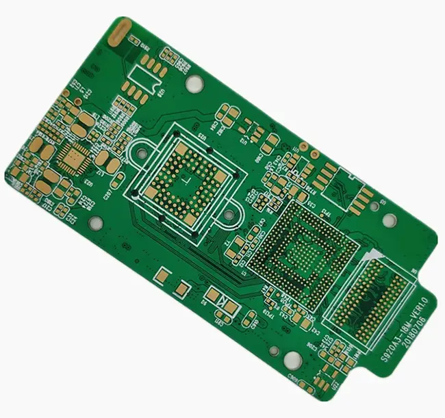
Description: Rigid PCBs is made of any structural material, from fiberglass, epoxy resin to any other. The board is stable and firm, showing no flexibility or conformity in the absence of rigidity or pressure. Rigid flex PCBs are primary applications that can be found in all electronic versions except where their robustness is a fundamental requirement, for example, in the automobile sector. Excellent performance with maximum rigidity makes it suitable for low-to-medium bags from applications with compressed geometry.
5. Flexible PCBs
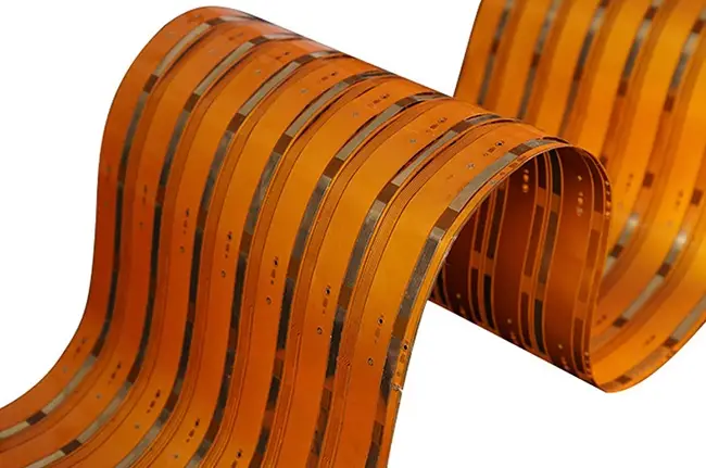
Flexible PCBs use flexible material and flexible substrates, which do not prohibit rigid flex boards from bending and conforming to convex contours. The narrow width will apply to devices with space restrictions or those that more frequently bend, such as wearables and medical devices. It is composed with flexible boards. Encourages small, lightweight designs and simplifies assembly procedures.
Rigid flex pcbs
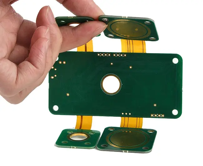
Flex rigid PCBs unite the properties of both rigid and flexible substrates. The resulting board has all the above benefits assembled in a single board. Present in devices having both relatively rigid and flexible zones, like smartphones with foldable display and aerospace technologies. Rigid flex PCBs bring ease of assembly, lessen cross linkage, and increases reliability.
7. High-Frequency PCBs
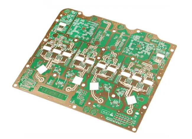
High-performance PCBs typically run signals at frequencies above 1 GHz. To achieve this, these boards generally feature exotic materials like PTFE (Teflon) that can handle these high frequencies. In telecom, aero, and high data-speed applications, Critical. It minimizes the signal loss, keeps integrity, and interfere interference.
8. High-Temperature PCBs
High-temperature PCB design utilize materials possessing the capacity to operate in highly elevated temperatures, usually above 130°C. It is remarkable in the automotive, aerospace, and industrial spheres that deal with extreme heat as a stimulus. Allows for efficient operation and longer life in severe environmental conditions.
9. Metal Core PCBs (MCPCBs)
In Printed Circuit Board with a metal core, the metal substrate (typically aluminum) develops heat much more efficiently as compared to surface mounting on the traditional substrates. All the scarce serum is used to treat people with rare disorders. Improves performance in heat transfer, ensures more extended lives for components, and provides higher reliability.
10. HDI PCBs (HD- Interconnect PCBs) are the High-Density Interconnect Printed Circuit Boards.
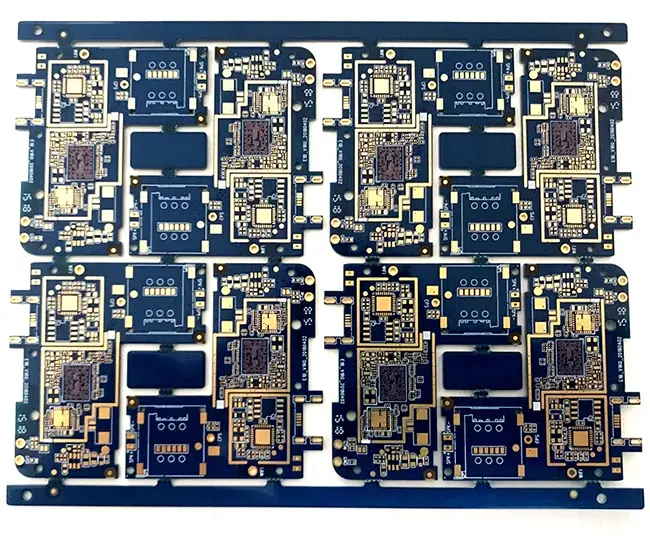
HDI Printed Circuit Boards apply advanced routing technologies, making possible a higher density of routing and smaller vias. This helps reduce the overall size of designs. Supercritical CO2 plays a vital role in the process of miniaturization of mobile phones, tablets, and other handheld gadgets. It shrinks the circuit footprint, provides signal integrity, and minimizes signal delay.
What are the Electronic Components of PCB Design?
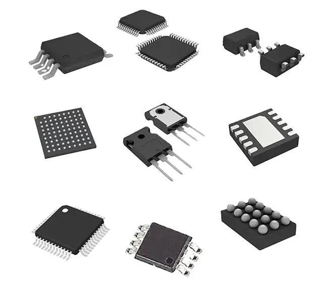
PCBs are principally made of a vast selection of electrically connected materials, which determine the functionality of the device in which the resulting board will be deployed. These PCB elements, such as transistors, fuses, resistors, and capacitors, are all required to create a functioning board, and they all make the device work properly. The components are soldered onto the pads of the board, which in turn are connected to the board circuitry. This allows components to be interconnected.
A board can be composed of one, two, or multiple layers of circuitry. If one of these devices breaks down or is damaged, the entire PCB fails to operate, and thus impairs the entire product’s functionality. On the other hand, why do they play such a significant role in our lives and in our society? Here are the five principal and vital PCBA key components done by their use and importance.
1. Resistors
Resistors are passive components that prevent the flow of electric current beyond their specified limits. They are used for voltage and current regulation in the circuit, to set biasing conditions, and to prevent damage to delicate components by excessive current.
2. Capacitors
The electron field is utilized to store the electrical energy in the capacitors. They are key devices in the process of smoothing out power sources, filtering noise, and providing temporary power in times of voltage drops.
3. Inductors
An inductor, more commonly known as a choke, is an electrical passive attach components, that is described as a coiled wire specially developed to enjoy this relationship by creating its own magnetic field, or it is utilized as a core to induce a magnetic field due to the current flowing through the coil. The magnetic field intensity of the coil, obtained from winding the copper wire into the author’s shape, is much higher than that produced by a single coil of wire.
4. Transistors
The transistor is a sophisticated semiconductor, that provides both the amplification and the flow of currents or voltages on a miniature scale, acting as a gate or switch for them. Therefore, it represents a nonlinear and active element in the conducting circuits. Often, transistors contain three multiple layers, two of which can hold current, while the third is bent in such a way that it helps the first two channels to connect or disconnect.
5. Transformers
Are the electrical devices that have a name plate marked in amperes that determines the amount of current drawn by the transformer. When current serves an AC circuit board, this electrical device is able to change the voltage level in a circuit. The reason is that they get power only from AC-based circuits and not from DC-based circuits. In the transformer, two coils are wound separately using a common core, in that both coils are the primary and secondary windings.
6. Diodes
A diode is a semiconductor with two terminals, where current flows in one direction. On one side, the end has high resistance, and on the other side, the end has low resistance. Diodes are used to clamp the voltage to protect the circuit and also keep DC out of AC. Two commonly used semiconductors include silicon and germanium, from which, diodes are made. Though they follow a unidirectional principle, the modes by which they transmit is distinguished. The category of diodes is divided into various kinds, and every kind has its own sphere of application.
7. Sensors
A sensor refers to equipment that generates an output signal to detect physical phenomena as they change.
In a general sense, a sensor is a device, module, machine, or subsystem that detects changes in the environment and sends the information to processors, where processors or computers usually transform the information into a suitable format for the user interface.
Structure and Application of PCBs
High-Density Interconnect (HDI) PCB Designs
The modern day equipment in PCB design continue to use HDI design practices, which entails advanced devices, smaller size features such as vias on the smallest PCB. Theses circuit boards have a rather familiar manufacturer process for circuit board design and production which utilizes more complex systems that needs more ranges of components and relations. Some of the well-known products where these circuits boards are used include:
Some of the well-known products where these circuits boards are used include: Smartphones and other mobile e-Devices, Add-in cards server and compute systems for UPS (uninterruptible power supply), Sink power directly from the main power line and Medical mini computers or micro implants that are almost impossible to detect.
Many of today’s microcontrollers, MPUs and FPGAs come in BGA configurations because this allows the least area of a multi-lead package, while still maintaining a large number of I/O pins. It is the BGAs that make the miniaturization in many devices and there are more consumer product that uses CUP in BGA packages.
Ultra-High Density Interconnect (UHDI) PCBs
The next stage of the PCB design and fabrication process features an integration with the chip packaging, which is responsible for the semiconductor chip hold in microcircuits. In the last processing chips they integrate on IC substrate where the PCB provides the interconnection between the electrical contact of the semiconductor die and PCB. In order to keep up with the development of ICs and achieve performance equal to that of IC substrates, the same manufacturing processes are used to make both IC substrates and UHDI PCBs.
What is Modern printed circuit boards?
Today, modern printed circuit boards (PCBs) play a crucial role as they are the core of all electronic devices including smartphones, computers, and many others. They have undergone a dramatic metamorphosis throughout the years, making them smaller, more powerful, and capable of managing intricate electronic circuits.
Layering: Application of multiple layers is nowadays possible therefore intricate circuitry can be achieved without increasing the physical size too much.
Materials: The materials implemented in the current PCBs are precisely selected for their electrical properties, strength and heat resistance.
Miniaturization: Integrating SMT and microvia drilling in production leads to the closely arranging electronic components on the modern printed circuit boards.
High-Speed Data Transmission: The present-day PCBs can deal with the high speed data transmission with very little data loss.
Flexibility: On modern electronics, Flexible PCBs (Flex PCBs) plays an increasingly important role, which is exemplified in applications, such as wearable devices and automotive electronics.
Advanced Features: Contemporary PCBs may even integrate onboard integrating components.
Environmental Considerations: Greenness of PCB manufacturing is gaining a momentum, with the use of materials and processes which are highly environmentally friendly and sustainable.
Understanding PCB Assembly
Printed Circuit Board assembly comprises of the procedure of soldering electronic components onto the printed circuit board. This procedure carries out a transformation of the green PCB with strips and dots determined as conductive tracks and pads into a fully operational electronic device. undefined
Types of Printed Circuit Board Assembly
- Surface Mount Technology (SMT): In SMT assembly, components are mounted directly on the surface of the PCB. This type of approach is preferred when dealing with components of smaller sizes, like resistors, capacitors, and ICs. SMT provides the advantages of higher component density, size reduction, low cost and improved electrical performance.
- Through-Hole Components (THT): The Through Hole Components Technology is a manual soldering of component leads through the holes of PCB and soldering them on another side. According to this approach, the laser cladding method is ideal for larger parts, connectors, and components that need mechanical strength. Though thermal heating treatment, or THT is not much used in electronic circuits nowadays, it is still employed for specific applications.
PCB Assembly Processes
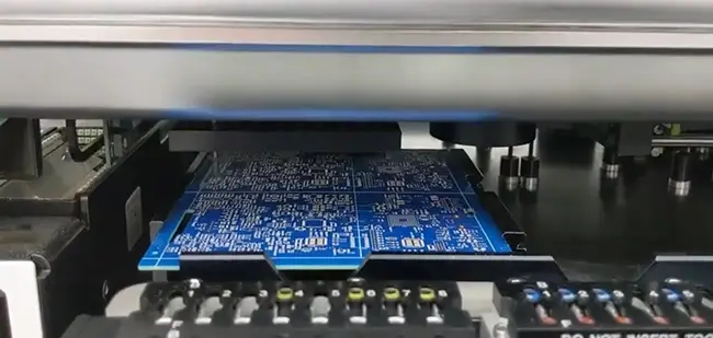
The PCB assembly process typically consists of several stages, each crucial for ensuring the final product’s functionality and reliability: The PCB assembly process typically consists of several stages, each crucial for ensuring the final product’s functionality and reliability:
Component Placement: In this stage, components are mounted onto the PCB using the instructions and specification of the design sheet. SMT line automated machines usually feature pick-and-place tools to achieve precise placement of electronic components.
Soldering: After the components are put in place, the next phase is soldering, which means making electrical links between the components and the printed board. SMT can be done using reflow ovens or SMT solder mask/wave soldering machines, and, through-hole Hole Component Technology can be done using THT soldering irons/wave soldering machines, or else reflow ovens.
Inspection: The completed assembly is inspected for any solder bridges, misaligned components, or soldering defects using X-rays, optical, or digital inspection devices. Frequently, AOI and X-ray inspection are the techniques used in an inspection process.
Testing: The PCB is then checked, to make sure all of the electronic parts are working the right way and there is no electrical fault. Functional testing, in-circuit testing (ICT), and boundary scanner testing are some of the methods used for testing.
Cleaning and Coating: Finally, the gathered Printed Circuit Board will go through the cleaning process to kill off the flux residues and other contaminants. Moreover, the conformal coating could serve the purpose of protecting the PCB from numerous elements such as moisture, dust, and corrosion as well.
Understanding the Manufacturing Processes of PCB
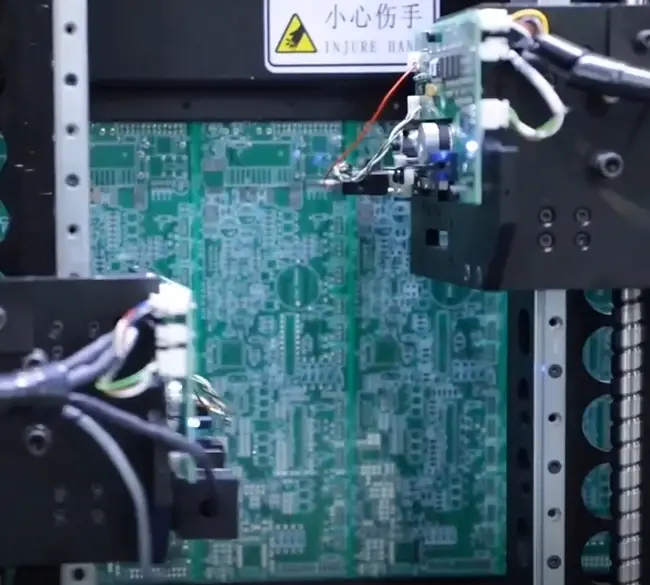
Printed Circuit Board utilizes very high pin count components which are assembled using a unique manufacturing process that involves specially made materials to support high copper shrink densities.
Design: With the help of the specialized software engineers are able to work on PCB design laying out the components, including component placement and trace routing.
Prototyping: A prototype PCB is developed and put to test for the purpose of detecting any design imperfections.
Production: When the prototype approved, mass production of PCBs can be brought about through the use of automated etching, drilling and soldering.
Quality Control: PCBs are put under very intense tests to ensure they are good conductors, work properly, and are strong.
Where are Printed Circuit Boards used?
Printed circuit boards (PCBs) are nowadays considered an essential feature of electronic circuits and devices, that make it possible to serve various sectors and application methods. PCBs are boards that connect electronic components. They are one of the most important components of the electronics that we encounter in our daily lives in a wide range of industries. They are implanted everywhere, starting from a cell phone to medical equipment, and this makes electronic parts available without the need for interconnection. Let’s be immersed in the wide world where the application of PCB is prevalent.
1. Consumer Electronics
Smartphones: Smartphones are constructed on the basis of single layer PCB layout which are a fabric on the boards of chips, processors, and connectivity modules.
Computers and Laptops: On the other hand, the single layer PCB in the different electronic devices, like the CPU, RAM, and storage devices, are responsible for transferring the data from one component to the other.
Televisions and Audio Systems: These gadgets depend on single layer PCB design for its signal processing, audio amplification, and therefore interface connectivity.
2. Automotive Industry:
Vehicle Control Systems: Contemporary cars deploy single layer PCBs on wide-scale for engine control units, sensors, entertainment, and protective technologies.
Electric Vehicles (EVs): An effective power management system in EVs relies on single layer PCBs for the control of the battery, engine, and on-board electronics.
3. Aerospace and Defense:
Aionics: Aircraft PCBs are used for navigating, communication, managing, and monitoring critical variables.
Military Applications: PCBs form the basis for radar systems, defense missile systems, encryption devices, and aviation equipment in defense technology.
4. Medical Devices:
Diagnostic Equipment: The primary purpose of PCBs is in powering medical imaging devices such as MRI machines and CT scanners as well as ultrasound systems.
Implantable Devices: As the backbone of pacemakers, insulin pumps, and other implantable medical devices, PCBs allow precise control and monitoring.
5. Industrial Automation:
Control Systems: Manufacturing facilities depend on PCB-based control systems for automation, processing and quality checking.
Robotics: PCB boards facilitate various operations in industrial robotics, such as motor control, sensor feedback, and data processing.
6. Communication and Networking:
Telecommunication Equipment: PCBs are widely employed in various networking links such as routers, switches, modems, and communication infrastructures, which are essential for data transmission and networking.
Wireless Devices: PCBs supply electrical connections to wireless communications devices like bluetooth speakers, wifi routers, & IoT components.
Renewable Energy Systems:
Solar Panels and Inverters: PCBs are being utilized in solar energy systems for functions such as converting power, monitoring, and control purposes.
Wind Turbines: PCBs are indispensable in wind turbines, since they maximize performance by inventing ways to make wind turbine functioning and monitoring effective.
8. Consumer Appliances:
Home Appliances: A printed circuit board is employed in such devices as refrigerators, washing machines, and microwaves, basically for control and user interface.
Smart Home Devices: Utilities such as smart thermostats, security cameras, and Internet of Things (IoT) devices in smart homes are dependent on PCBs.
In Conclusion
Printed Circuit Boards remain the cornerstone of modern-day electronics devices in terms of functionality and innovation. Their diversity, integration, and scalability make them incomparable values for the whole human society, from consumer electronics to aerospace. Comprehending the complexities of PCBs besides makes our technology enjoyment meaningful but, importantly, reaffirms their place in our web-connected scenario.


One Response