HDI PCB
Flexible Order Quantities
We offer HDI PCB production with no minimum order quantity, ensuring flexibility and cost-effectiveness for all project sizes.
Rapid Prototyping and Production
- Sample: 3-5 Days
- Mass production:8-10 Days
Advanced Layering and High Density
- Layers:4-32
- Versatile Layer Interconnectivity
Expert Technical Support
- One-on-one engineering services
- 24/7 Customer Service Online
- Flexible design
Take a peek inside our COMPREHENSIVE GUIDE
What is a HDI PCB?
HDI PCB, or High-Density Interconnect Printed Circuit Board, is a type of PCB that offers higher wiring density per unit area compared to traditional PCBs. This increased density is achieved through the use of finer lines and spaces, smaller vias and capture pads, and higher connection pad density. HDI PCBs are characterized by their ability to include more components in a smaller area, making them ideal for modern, compact electronic device
Key Features of HDI PCBs
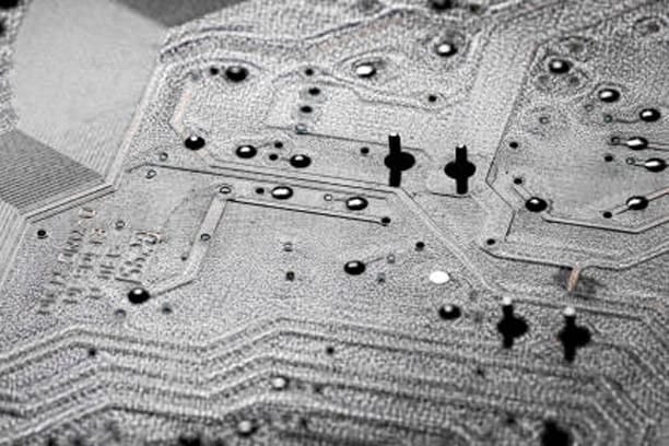
These are very small vias with diameters typically less than 150 microns, which connect the different layers of the PCB. Microvias help reduce the space required for interconnections, allowing for more compact designs.
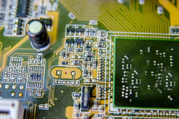
HDI PCBs often utilize blind and buried vias. Blind vias connect an outer layer to one or more inner layers without passing through the entire board, while buried vias connect only internal layers.
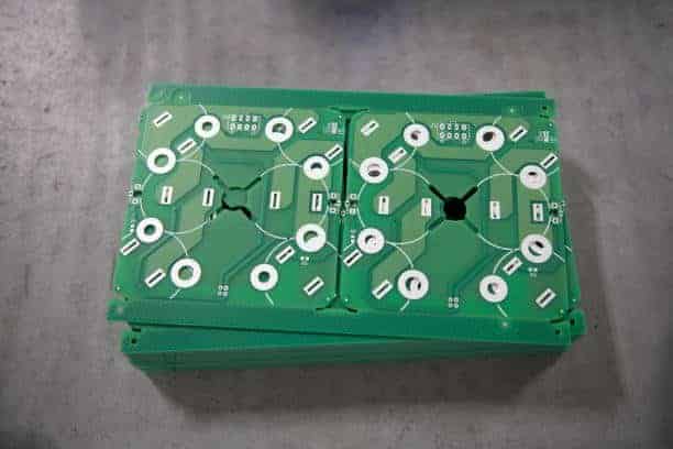
HDI PCBs can have a higher number of layers compared to conventional PCBs, supporting more complex circuitry. This allows for the integration of advanced features and functionalities in a single board.
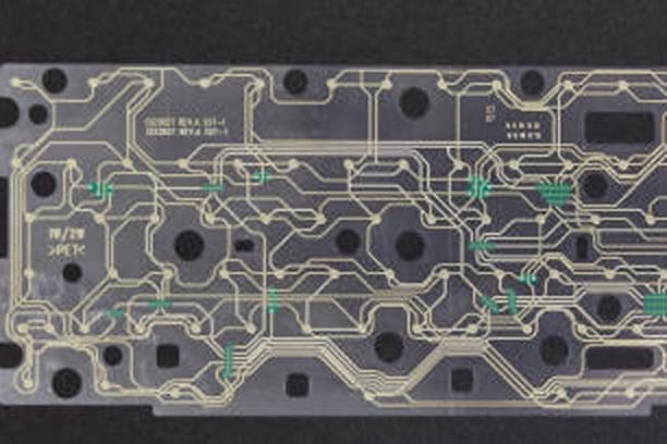
HDI PCBs use thinner materials, which contribute to their compact size and lightweight nature. This is crucial for applications where space and weight are critical considerations.
HDI PCB Board Design and Manufacturing Processes
High-Density Interconnect (HDI) PCBs are a type of printed circuit board with a higher wiring density per unit area compared to traditional PCBs. They achieve this through the use of finer lines and spaces, smaller vias and capture pads, and higher connection pad density. HDI PCBs are essential for modern electronics that require compact designs with high performance, such as smartphones, tablets, and other high-speed digital devices. Here is an overview of the design and manufacturing processes of HDI PCBs:
HDI PCB Design Process
Requirement Analysis
Define the specifications, including layer count, materials, impedance control, and electrical/mechanical requirements.
Stackup Design
- Determine the layer stackup, which includes the number of layers, material selection, and thickness of each layer. HDI stackups often involve microvia layers, buried vias, and sequential lamination processes.
Component Placement
- Place components strategically to optimize space, thermal management, and signal integrity. HDI PCBs allow for closer placement of components due to finer lines and spaces.
Routing
- Use advanced routing techniques such as blind and buried vias, microvias, and via-in-pad to achieve high-density interconnects. High-frequency signal lines may require controlled impedance routing.
Design for Manufacturability (DFM)
- Ensure the design meets manufacturing capabilities and constraints. This includes considerations for drill sizes, aspect ratios, annular ring sizes, and tolerances.
Simulation and Verification
- Perform electrical and thermal simulations to verify signal integrity, power integrity, and thermal performance. Tools like SPICE, SI analysis, and thermal analysis software are commonly used.
HDI PCB Manufacturing Process
Lamination
- Core Lamination: A central core material is laminated with copper on both sides.
- Sequential Lamination: Multiple layers are built up sequentially, often with dielectric materials and copper foils laminated together.
Drilling
- Laser Drilling: Used for creating microvias, which are small holes that connect adjacent layers. Lasers can achieve high precision and small diameters.
- Mechanical Drilling: Used for larger vias and through-holes.
Desmearing and Plating
- Desmearing: Removes resin smear from the drilled holes.
- Electroless Copper Plating: Deposits a thin layer of copper inside the vias and on the hole walls.
Patterning
- Photoresist Application: A photosensitive resist is applied to the copper surface.
- Exposure and Development: UV light is used to expose the desired pattern. The unexposed resist is then developed away, leaving the pattern for copper etching.
- Etching: Removes unwanted copper, leaving the desired circuit patterns.
Copper Plating and Solder Mask
- Copper Plating: Additional copper plating to increase the thickness of the traces and vias.
- Solder Mask Application: A protective layer that covers the PCB surface except for the pads where components will be soldered.
Surface Finish
- Surface Finishes: Various finishes like ENIG (Electroless Nickel Immersion Gold), OSP (Organic Solderability Preservative), or HASL (Hot Air Solder Leveling) are applied to protect the copper pads and ensure solderability.
Silkscreen Printing
- Silkscreen: Text and symbols are printed on the PCB for component identification and assembly instructions.
Testing and Inspection
- Electrical Testing: Tests for continuity and isolation to ensure all connections are correct.
- Automated Optical Inspection (AOI): Inspects for defects in the traces, pads, and solder mask.
- X-ray Inspection: Used to inspect hidden vias and internal layers.
Key Applications of Automotive PCBs
- Enhanced Performance
HDI PCBs provide better electrical performance due to shorter signal paths and lower inductance and capacitance. This results in faster signal transmission and reduced signal loss, making them suitable for high-speed and high-frequency applications.
- Miniaturization
The ability to pack more components into a smaller area enables the miniaturization of electronic devices. HDI PCBs are essential for the development of compact gadgets such as smartphones, tablets, and wearable technology.
- Improved Reliability
The advanced manufacturing techniques used in HDI PCBs result in improved reliability and durability. The use of microvias and reduced number of solder joints minimize the risk of mechanical failures and improve the overall robustness of the PCB.
- Increased Design Flexibility
HDI technology offers greater design flexibility, allowing for the creation of complex and innovative electronic products. Designers can incorporate more features and functionalities without compromising on size or performance.
Applications of HDI PCBs

Consumer Electronics

Automotive Industry
Medical Devices

Aerospace and Defense
HDI PCBs represent a significant advancement in PCB technology, offering numerous benefits in terms of performance, miniaturization, and design flexibility. Their application spans various industries, driving innovation and enabling the development of cutting-edge electronic devices. As technology continues to evolve, HDI PCBs will play an increasingly vital role in shaping the future of electronics.

