Delve into depths of PCB layout to learn about adding Via-in-Pad structures in our step-by-step guide. Understand the basic components and how to insert them into your assembly and production systems in a smooth way. Take advantage of the capabilities of the PCB designs and make the manufacturing process much more efficient by realizing experts ideas and limited to practical features. Leverage the full Via-in-Pad integration capability to achieve a new dimetion of performance in your electronic compositions.
What is a Via-in-Pad?
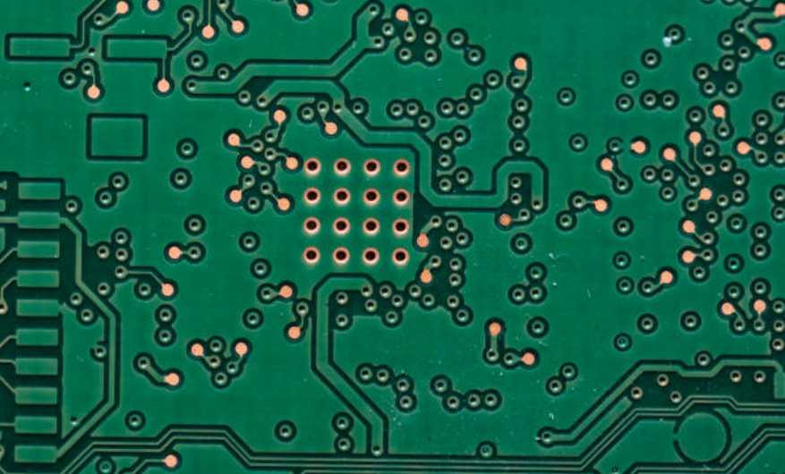
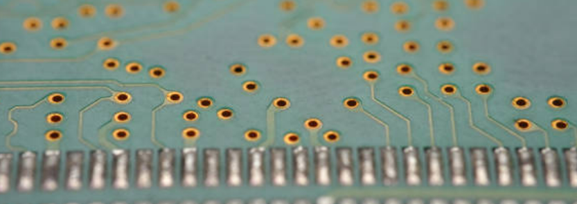
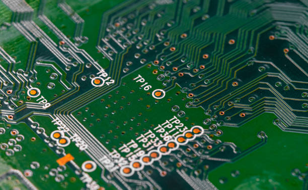
A VIP or via-in-pad (VIP) is a design technique which creates such layered structure in printed circuit boards (PCBs) that a via (a plated-through hole) is situated within the pad of a surface-mounted device. With this technique, the PCB can be designed in a more compact manner and thus space on the board can be used better, as long as the vias are produced out of the conventional surface area.
Via-in-Pad structures are preferred widely during the high-density PCB design especially in applications like limited space or where signal quality is critical. The impairment of the signal paths is the unwanted effect but through placing the vias directly into the other vias in the same via in pad design, the lengths of the signal paths are shortened, and the impedance is reduced resulting in better electrical performance. Other than that, VIPs can also bring higher thermal conductivity and dependability, especially used in the designs where the achievment of high heat dissipation is necessary. In general, vias-in-pad take various merits into account modern technology of the printed circuit board assembly processes.
Designing Via-in-Pads
Via-in-Pads (VIPs) designing is an essential part of PCB designs for high-density printed circuit board (PCB) which is used in products like smartphones where miniaturization is the key feature. VIPs can reduce the layout density blind vias in a PCB by enabling the orientations of vias underneath the pads of surface-mounted components.Here’s a step-by-step guide to designing VIPs:
- Determine the Need: The VIPs highly utilized in locations where space is scarce or in processing high-speed signal lines, respectively. Evaluate your design scheme to know whether VIPs are key for your design.
- PCB Layer Stackup: Ensure that VIP stackup is fitted for your PCB. VIPs might explicitly use the layer-arrangement and materials drop that are intended to support the signal integrity and manufacturability.
- Component Selection: Pick components that are compatible with VIPs. It is not mandatory for all the components to VIP designs due to the small pad sizes and components which is negatively affected by the reflow soldering temperature.
- Via Size and Placement: Establish which path to use and place it as well. It must be small enough to fit within the via but large enough for proper thermal pads dissipation and electrical conductivity. Planning the via layout should be done with the goal to achieve the signal integrity and the category of the production.
- Design Rules: Establish design guidelines for VIPs. Areas to incorporate include minimum via-to-via spacing, via-to-pad clearance, and via aspect ratio to achieve high performance and manufacturing capability.
- Thermal Considerations: Evaluate thermal aspects, first of all for heat-pad components. VIPS can affect heat dissipation, so thermal pad management allocation should definitely be provided in order to prevent overheating.
- Signal Integrity Analysis: Define signal integrity analysis of VIPs to investigate the influence of signal quality. Equipment featuring electromagnetic simulations can be used to detect and alleviate problems associated with VIPs’ signal integrity.
- Manufacturability: Collaborate with PCB Manufacturer to the last details to check manufacturability. For VIPs it may require special fabrication techniques like laser drilling and/or via filling, please be specific when you instruct your needs and requirements.
- Documentation: VIP processing of documents in the PCB design files. Issuing detailed instructions both in the form of diagrams and notes to the manufacturer is necessary for manufacturing and assembling the finished product correctly.
- Testing and Validation: Assessing and validating VIPs’ performance for their effectiveness. Test signalling, thermal, and continuity conditions that electrical standards meet the design criteria.
Via in pad PCB Fabrication Process
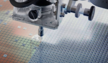
One of the common process in via in pad PCB design fabrication is via in pad, where creating small holes accross pads of surface mounted components is involved. This position happens to be closer to the surface routing the board, in this way the size of the mounted print circuit board is decreased and the signal integrity is improved.
The process typically involves the following steps:
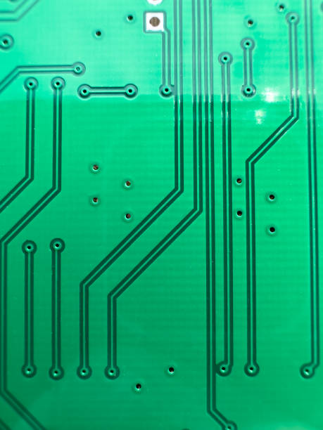
- Design: The PCB designed is the stacked via pads layout. Here, we emphasize on working out the exact dimensions of the vias, and any extra design aspects, like impedance control or thermal management.
- Drilling: Through these processes, small holes get drilled into the pads of the surface mount components by a laser or by mechanical drilling methods. These gaps are normally filled with conductors, a normal example being copper, to provide electrical connection.
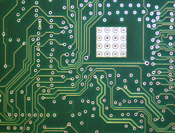
- Plating: Vias are drilled through the PCB after drilling before plated to complete the conductive connection between the component pad and the rest of the PCB. It is even possible here to use techniques like electroplating or chemical deposition.
- Solder mask application: A solder mask goes across the surface of the prototype PCB to guard it from external conditions and civil disobedience. Through-holes in the pad may be filled with non-conductive material which will stop the flow of the solder into the holes during process of assembly.
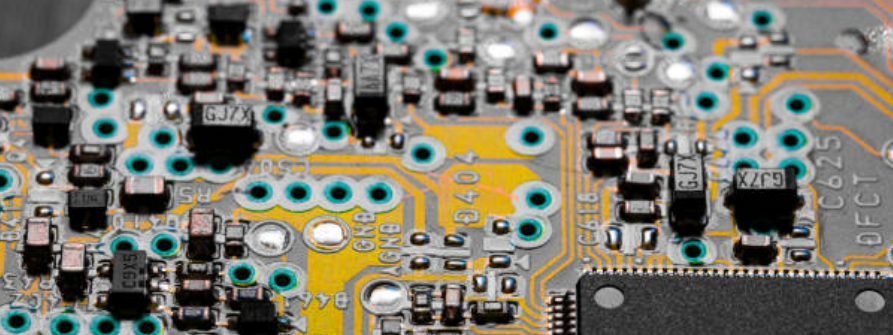
- Component assembly: Surface mount components are next applied to PCB by a solder paste and reflow soldering process. The vias in the through-holes offer a direct connection between the component and the printed circuit board tracks which prevents the necessity of other vias on the board.
Fundamentally the VIA in pad PCB fabrication process allows for more electronic components to be put in a smaller space which boosts signal integrity and results in a smaller form factor rendering the VIA in pad ideal for electronic devices which are compact, finished quickly and high performing.
Potential Applications for Via-in-Pad
- High-density PCB designs: The use of via-in-pad technology permits a higher pack density on the PCB, which makes the latter suitable for applications with limited space.
- High-speed and high-frequency applications: Via-in-the-pad technique enables to minimize signal loss and impedance transformation, making it ideal for high-speed and high-frequency applications where a signal quality is critical.
- BGA (Ball Grid Array) packages: Via-in-pad technology can be used for a direct BGA pads’ interlayer connection, improving thermal characteristics and attainability.
- RF and microwave applications: The via-in-pad approach securely design the controlled-impedance vias that suit RF and microwave unit in the applications, optimize the signal transmission thus.
- Thermal management: Via-in-pad technology able to give thermal dissonance a boost by establishing a direct connection between thermal vias and pads, thus promoting the dissipation of heat away from various components.
- PoP (Package on Package) assemblies: The tandem-in-pad technology can be used for stacked components on pins and capabilities of PoP (Package-on-Package) assemblies, reducing space and enhancing signal integrity.
- HDI (High-Density Interconnect) PCBs: The technology called via-in-pad is applied in HDI PCBs to make more alternative routing and whereby raise design freedom.
- LED lighting: Through the leaded purpose, LEDs may be just connected to the circuit board that ensures good thermal behaviour as well as surfers the production costs.
- Wearable devices: Through the Via-in-pad technology, along with the compact and lightweight attribute of the wearable devices, it becomes easily possible for the signal transmission to be maintained with a little or no interference leading to the improved outcome.
Via-in-Pads in Internal Layers
Vias in pads (VIP) on the inner layers of PCBs can be a heat breaking but the time and space consuming solution for high density interconnections and efficient routing of complex designs with many layers. However, there are several considerations to keep in mind when implementing VIP technology on internal layers:
Signal Integrity
The via placement in vias on internal layers can result in bad signal integrity, if it occurs on pads, especially for high-speed applications. The instance of signal reflections also merges with impedance discontinuities at through hole vias when the transition between the via and the pad run at the end like this is possible to be a bad signal worsening Engineers must take INR into account traditional routing methods and may have to install certain routing techniques including controlled impedance routing or functional simulations as a way of reducing the impact from these problems.
Thermal Pad Management
VIP can be used on internal layers very successfully. However, it is important that thermal management can be carried out if vias are carrying significant current or if the components on the external layers generate heat. Specific thermal vias should be used to make heat management create a thorough thermal relief scheme, effectively dispersing heat from the hot deck critical components.
Manufacturability
The interconnection of vias in the internal pads is more difficult than by the electroless plating processes which are connected to the external layers. Designers should closely consult with PCB manufacturers to confirm if fabrication is a practical option and it can actually provide VIP structures on internal layers.
Layer Stacking
VIP maximizing the layer stacking, both on the internal and terminal layers, could also be used. The designers are required to apply appropriate location of pads that shares the space with signal traces, power planes or with the ground planes from adjacent layers in order to be strong electromagnetic interference and crosstalk free.
Material Selection
The selection of materials for internal layers stands out the most as it determines the electrical and thermal performance of the resultant device. Lossless dielectric materials that are good heat conductor may be put on the inner production of the PCB to reduce the signal attenuation and efficiently discharge the heat.
Routing Density
The VIP on internal layers helps achieve higher routing density and more compact designs in which vias can be positioned directly under the component pads. Thus, the designer should take an advantage of this capability and arrange the wiring for minimum loading and delay droppings.
In general, the insertion of vias in internal pads can bring about a wide range of advantages regarding routing density and design efficiency; however, it is critical to pay attention to the issues including signal integrity, thermal management, manufacturability and material selection of thermal pads in order to maintain the reliability and performance of PCB. Partnership between designers and PCB fabricators results in the effective checkmark of design issues promptly, and hence, the implementation of VIP technology including the buried vias on internal layers will succeed.
Via in pad application for SMD Pads
Plated vias in pad technology is a technique with SMT allows vias to be located directly under the solder mask of component’s pad. This practice, in turn, increases the space without compromising the quality of the board signals as it shortens the trace length pad size of the via.
To apply via in pad technology for SMD pads, follow these steps:
- Develop PCB layout with the reference design of vias in the center of SMD pad. Solder the component afterwards on the SMD pad.
- For the PCB Board design choose the software that may enable the via structures in pads of SMD pads.
- Strictly adhere to well-placed and sized vias of vias in pads technology, which are in compliance with the manufacture’s specifications for the technology.
- Design the pcb pads and SMD pads carrying the vias via high-precision PCB fabrication to guarantee the actuality of the placement.
- Proceed to reflow the solder paste after securing the components on the PCB’s surface to make sure that the material is completely around the vias in the pad.
- Measuring the solder joint integrity after assembly is important for all the pads vias technology to have been utilized.
- Inspect whether the solder joints are reliable or not after the assembly, verify that the vias in pad technology had been assembled correctly.
These instructions show you how to spaced pad via in pad technology smd pads on your PCB use via in pad design to save space and to improve signal integrity.
Examples of Via-in-Pad Usage
- BGA (Ball Grid Array) packages: The thru-hole type BGA package uses via-in-pad technology. This ensures high interconnectivity between the package and PCB.
- High-speed PCBs: Via-in-pad technology is frequently utilized in high-speed PCB layouts to cut down on the extent of the signal distortion and thus improve signal integrity.
- RF applications: Via-in-pad technology is widely implemented in RF applications as it provides a low-resistance path linking the parts successfully.
- Miniaturized devices: Via-in-pad technology is greatly useful because it can decrease the size of the PCB and save the footprint space of the devices such as wearable ones.
- High-density PCBs: The via-in-pad tech is a game-changer for the designers. Because of the fact that more connections are possible in the confines of a small area, this technology reduces the need of the component density.
- High-frequency applications: Transmission through pads featuring Via-in-pad technology may considerably reduce the signal loss and improve its quality in applications with high frequency.
Conclusion
Via-in-pad (VIP) technology provides lots of benefits to printing circuit board design in terms of space saving and routing optimization, especially in the case of high-density applications. Via-in-pad technology is a unique technique that routes channels directly beneath the component’s pads. This approach allows for a smaller circuit board footprint and improved electrical performance. Although VIP introduces such features as signal integrity, thermal management, manufacturability, material selection, routing density it gives more complexity to the implementation process. The collaboration with designers and PCB manufacturers is of fundamental importance for By the way, untangling these aspects is mandatory and the quality and performance of the VIP capable PCBs has to be guaranteed. However this technology might face some difficulties yet it is an amazing innovation that makes a great contribution to the level of modern devices and ability to be compact and advanced.