Discover definitively the power of PCB and other testing methods with our thorough walk-through, enriched with specialist insights, advanced strategies, and handy hints, guaranteeing that you will acquire mastery in the electronics evaluation. Investigate such testing methods for testing continuity, insulation resistance, functionality and other important parameters, that are required for your printed circuit boards quality and reliability. Irrespective of whether you are a veteran engineer or a top initiate this ultimate guide will give you power over your testing juice and you will improve on you projects until they become a superior class of performance and durability.
WHAT IS PRINTED CIRCUIT BOARD (PCB) TESTING?

PCB testing, also known as printed circuit board testing, circuit board test qualifications is meant to determine whether PCBs function well, are of good quality, and are reliable. PCBs, crucial elements of electronic facilities, provide mechanical support and electrical contacting for the most parts of electronics in the application of them. The testing of printed circuit boards (PCBs) is noteworthy for the purpose that they must conform with the design specification, should perform reliably, free from any errors or faults before they are deployed in the various electronic products.
OBJECTIVES OF PCB TESTING
The objectives of Printed Circuit Board testing and verification are many-sided, whereas they intend to test points verify that PCBs are sound, reliable, and work properly. Here are the primary objectives of printed circuit board testing and verification:
- Quality Assurance: Printed Circuit Board testing and verification is the best way to know that the manufacturing process has been achieved successfully and that the PCBs are surely meeting the quality standards and the design specification. It reveals any problem being caused by production, assembly, or its usage, respectively.
- Fault Detection: PCB tester resolves and identifies failures, defects or aberrations in the board including a possible short circuit on the board, component defect or poor connectivity. Electrical automation comprises identifying the problems of de-soldering, open circuits, short circuits, component shortcomings, or manufacturing defects.
- PCB Functional Test Verification: Printed Circuit Board testing and verification will confirm that the PCB performs its designated task well and without any dropouts. It does that, meaning there are no conductor malfunctions, signal runs, and other components as they are set out to perform required parameters.
- Reliability Assessment: The reliability and durability of the PCB can be determined through PCB testing by simulating varying operational conditions and external stresses. It assesses the PCB’s response to a sustained application of temperature members, humidity, vibration, and shock over a reference life of the PCB.
- Compliance and Standards Conformance: Printed Circuit Board testing and verification provides information to the end users that it fully complies the industry standards, regulatory requirements, and customers’ specifications. This provides an evidence that the PCB is indeed safe quality with regard to the applicable EMC, and other regulatory standards that may apply to the intended use and application.
- Cost Reduction: The testing of PCBs assists the identification of and solving of issues at an early stage of the manufacturing process. Thus, reworking, scrap materials, and, hence, the popularity of warranties related to defective PCB are minimized. It optimizes manufacturing production by saving expensive components and by process monitoring.
- Customer Satisfaction: Printed Circuit Board testing and verification is aimed at guaranteeing the product quality satisfies and even exceeds customers’ requirements for accuracy, reliability, and dependability. It improves customer satisfaction by the means of ensuring that they avail of fail-proof electronic products which come in a variety to meet different customers’ needs.
Through accomplishing these goals, Printed Circuit Board testing and verification serve the purpose to support the burn in testing the quality, reliability and achieving the general success of electrical products, which finally should meet the expectations and requirements of users and all stakeholders.
TYPES OF PCB TESTING METHODS
Here are the primary types of Printed Circuit Board testing and verification equipment that employs various testing methods to ensure the quality, reliability, and functionality of printed circuit boards (PCBs):
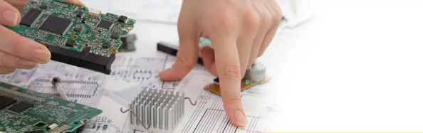
Visual Inspection
Visual inspection means to scan the PCB visually for a number of defects including misalignment of components, damages, wrong soldering, etc. An initial approach with PCB testing procedures is also a manual visual inspection performed mostly in manners either a manually or taking advantage of optical inspection systems that are automated (AOI).
Continuity Testing
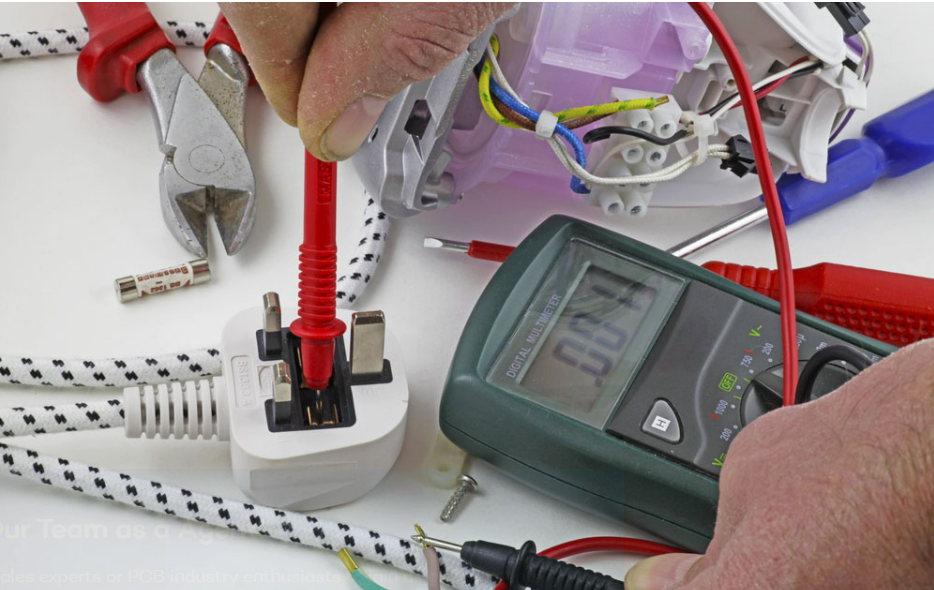
Continuity testing guarantees that the PCB serves the right connections in their in-circuit testing, ensures that all contacts are perfect and there’s no open circuit, among other things. The measurement can be done by multimeter, which utilizes the automatic part in circuit testing equipment.
Insulation Resistance Testing
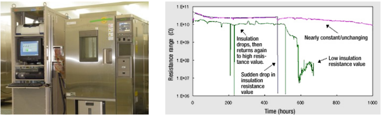
Insulation resistance is a way of assessing the resistance between the conductive flux and the board’s insulation material. Whether for monitoring a warehouse’s load capacity, network status or connecting the sensors in an industrial application, it eliminates any faults that might get in the way.
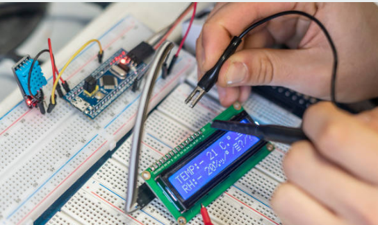
Functional Testing
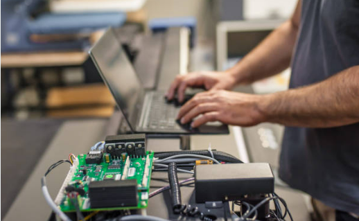
PCB Functional testing ensures that the circuit board is operated in the usual manner and also performs its functions perfectly where there are no faults arising. In doing this, it might result to functionality tests which can be the application of power to the board or testing its outputs and/or interfaces by a repeated measures experiment under different operating environment conditions or in multiple times.
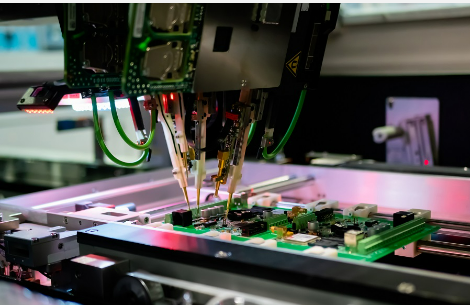
In-Circuit Testing (ICT)
ICT includes in circuit testing and pathways at individual component mass on the PCB using ICT testing as the components are still mounted on the board. It is the one that isolates and detects failures in components or defects on the fly, a vital testing method for the production lines with high volumes.
Flying Probe Testing
Flying test probe of automation probes components and interconnection of the circuit board, no need to custom test fixture, hence, during the flying test probe no need for the custom test fixture. It is a useful tool for testing prototype and low-volume PCB designs and can be quickly adapted and extended to new PCB designs.
Boundary Scan Testing
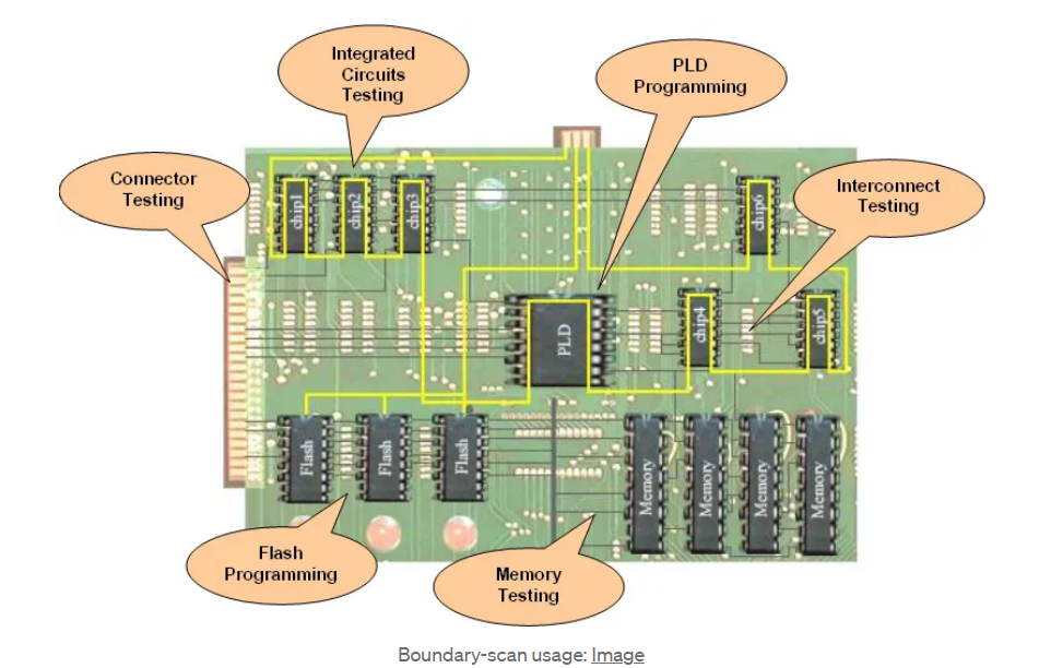
With boundary scan testing, there is a special kind of testing technique which uses the test logic circuits built-into the PCB to check out the connectivity of digital pathways and devices on the board. It is functional test especially ideal for customization of multi-layer, compact PCB that carries many digital components.
X-Ray Testing
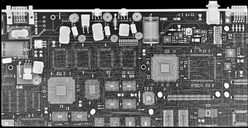
X-ray testing in PCB boards is known by various names such as X-ray inspection, or X-ray analysis. It is deployed as a non-destructive testing method to examine the inner structure of the conductors and detect solder joint defects for example, that may look normal from the exterior.
Environmental Testing
Environmental stressing mimics real-life environmental conditions like temperature, humidity, vibrations, thermal stress, and mechanical shock to test and check the improvement in performance and reliability of PCBs as operating environments.
Such PCB functional testing methods can either be used individually or in certain sequences which are dependent on the type of PCB material and the specific aims of the testing. Through their consequent use these testing approach enables manufacturers to achieve quality, reliability, and, in the end product, an improved level of performance leading to satisfaction of clients.
IMPORTANCE AND BENEFITS OF PCB TESTING
The contribution of the functional testing in the improvement of the efficiency of printed circuit boards (PCBs) is eternal, and functional test is regularly used as vital tools in giving PCBs reliable and avenue for customization. Here’s why PCB testing is crucial:
- Quality Assurance: PCB testing proves by itself that all instructed design specifications and quality criteria are done with the same electronic product, securing its uniformity and reliability.
- Defect Detection: By predicting the defects early in the PCB manufacturing process, it decreases the final number of non-operational boards reaching the assembly stage, minimizing the costs for scrap, rework and repairs.
- Reliability Enhancement: Through rigorous testing we have managed to narrow down and detect prospective reliability issues including bad solder joints and parts failures before they become a problem in a product and cause a field failure.
- Compliance Verification: PCB testing means that products may be assured to comply with the industry standards, the regulatory requirements, and client preferences, and under such condition, they can all be deemed to be safe, reliable and high performing.
- Cost Reduction: The PCB test enables you to detect and address defects early on, which in turn leads to minimized rework cost, scrapping, and warranty repairs. Thus, you can lower the production cost and increase profit itself.
- Customer Satisfaction: Excellent PCBs are good for the production of long –lasting and reliable products, on which customers rely to meet or over-perform their expectations, eventually creating a good reputation and satisfaction of customers
- Process Improvement: Data analysis from the PCB testing enables manufacturing plants to know more about their processes, allowing the improvement efforts that focus on quality, efficiency, reliability, and all aspects of the manufacturing plant so as to facilitate its improvement.
- Risk Mitigation: PCB testing will address thebrand issues arising from product recall, warranty claim, and product failure that result in poorrepair of the brand.
- Market Competitiveness: Quality PCBs can be relatively produced through strict quality inspections while these so the company gains its competitiveness in the market, customers prioritize quality and reliability.
- Long-term Performance: The reliable PCB’s endeavors allow for long term performance and resilience of an electronic device that shortens the downtime, repair costs, and its customer dissatisfaction.
PCB testing is a crucial part of guaranteeing that electronic products meet the required standard in terms of quality, dependability, and performance. Producers, customers, and other stakeholders both benefit from conducting this type of test. Through investment in proper testing and state of the art in initial to meet with the expected quality is the main market requirement, manufacturers can deliver smartly which are the highest even in the current demanding market.
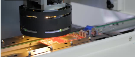
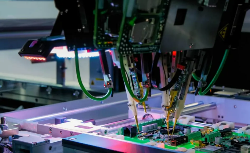
HOW AUTOMATED OPTICAL INSPECTION (AOI) WORKS IN PCB TESTS
In PCB testing there exist a state-of-the-art procedure certified for finding errors called Automated Optical Inspection (AOI).
- Preparation:
- The PCB is usually cleaned before examination to avoid any kind of contaminants that could spoil the inspection process.
- PCB can be submitted to a pre-scan alignment process to validate proper alignment and imaging of the board, as the next step.
- Image Acquisition:
- The PCB will be placed in the automated optical inspection system’s x-ray inspection platform after being transferred.
- High-resolution cameras with specialized lenses that have top-quality lenses and can produce images from different aspects and perspectives take photos of the PCB.
- The fabrication process involves taking multiple images to cover the entire surface of the PCB both the sides if required.
- Image Processing:
- The images taken by the observatory are processed and analyzed by the high-end testing software algorithms.
- The software compares the images with the reference image or the CAD data of PCB design that was provided.
- Defects may include missing parts, misaligned parts, soldering defects (such as bridging or poor contacts), and incorrect polarities, which are defined based on visually visible deviations from the reference image.
- Defect Detection:
- The automated optical inspection technology brings the inspection into a new level by detecting and then categorizing the fault based on the specific model and inspection rule.
- It divides whether the critical defects raise and then the non-critical defects that may probably be in a further stage of the analysis, review or monitoring.
- Reporting and Analysis:
- The Automated Optical Inspection (AOI) system gather specific visual data, showing the exact location and the type of the found defects.
- Inspection data is kept in a traceable database where it is reported together with also some stats and also images of defects.
- Manufacturers are able to monitor inspection outcomes for finding patterns, controlling the process mechanics, and increasing production throughput.
- Decision Making:
- Inspector reports of that inspection will give to manufacturers some recommendations to be used in the determination of the PCBs disposal.
- Faulty PCBs are reworked again to help discover and fix the defects or they are discarded completely if the defects are too extensive to be repaired.
- Feedback Loop:
- AOI systems offer process feedback sensing which in turn ensures the manufacture process has real-time output which eventually enhances the quality and reliability.
- Ongoing monitoring and analysis of the Automated Optical Inspection (AOI) data give manufacturers the possibility to find out what steps should be eliminated and in which point of the process some mistakes happen.
In general, AOI contributes highly to PCB functional testing methods through its precise, high-speed and complete inspection of the PCB at the manufacturing or production stage. It also is final quality control procedure contributes to strict quality control, lowers manufacturing cost and facilitates the processing of superior electronic items.
DIFFERENCE BETWEEN PCB TESTING AND TEST ANALYSIS
PCB testing and test analysis are concerned with fixing and curbing the defective products thus both are indissolubly linked under the umbrella of quality assurance and quality control.Here’s how they differ:
PCB Testing
- PCB testing involves manual checking of the boards through visual and electrical evaluation which aims to ascertain quality, dependability and functionality requirements of the boards.
- It stands for several processes spanning from the visual observation to functional testing including continuity testing, insulation resistance testing among others.
- The main purpose of PCB testing is to find defects, irregularities, or mismatches in the PCBs themselves, including such electronics issues as double soldering, component misalignment, open circuits, or short circuits, or incorrect placement.
- The main objective of PCB testing is to ensure that the PCB follows the design specifications, gives the desired performance, it is of the right quality to be deployed in electronics products.
Test Analysis
- Test analysis, in contrast, involves checking and interpreting the test data that is obtained during the PCB testing procedures.
- It is the technique of reviewing various test data for analyzing patterns, trends or anomalies and extracting meaningful insights into the reason why certain aspects go wrong and how to enhance the manufacturing processes, product quality or reliability.
- Test analysis can be performed by different means like statistical analysis, data visualization, root cause analysis, failure analysis, and several others to know what is actually the cause of failures or defects noticed during testing.
- The main objectives of test analysis are to draw more insightful inferences regarding the performance and behavior of PCBs, spot the room for facilitating a transformation process, and make the right selection for improvement.
In general, the PCB inspection is a physical examination of PCBs to detect defects, whereas test analysis concerns the analysis of test data by finding meaningful information to enhance manufacturing processes. They are inseparable entities of the manufacturing process and the enablers of quality assurance and quality control in PCB and production process, which in turn guarantee the production of precise and reliable electronic goods.
CHALLENGES IN PCB TESTING
PCB testing entails tremendous structural complexity of a contemporary electronics and a PCB scheme reflecting the designs and manufacturing processes. Here are some common challenges in PCB testing:Here are some common challenges in PCB testing:
- Miniaturization: With the continuing progression of device miniaturization and PCBs increasingly densely populated by components, this makes it progressively harder to reach and examine individual components and connections.
- High Component Density: For high-density PCBs with many components and fine traces all together, it is hard for the traditional testing to check the correctness and analysis accurately and thoroughly.
- Complexity of PCB Designs: Today’s PCB designs could often be very complicated, contain multi-layers and fast speed signal paths, and it is not easy to test these PCBs properly covering all aspects of this PCB.
- Variability in Components: Characteristic of every component can be different, like tolerance, manufacturing process, and counterfeit parts, that can a affect accuracy and reliability of test.
- Intermittent Faults: Complications caused by intermittent faults where the problem appears in a rare occasion or under certain condition are hard to discover and diagnose using traditional test. Therefore, new PCB functional testing methods are needed to find the cause of such problems.
- Testing Cost and Time: Comprehensive testing of PCB circuitry often involve tedious and expensive procedures that become a hurdle for large volumes production runs, thus ballooning the production period and adding up the cost of manufacturing.
- Adaptability to New Technologies: A major challenge that has been posed to the techniques of testing is the exponential increase in the technology, for instance, the new component types, materials, and manufacturing processes. Therefore, continuous innovation and adaptation are important tasks that must be done to keep pace with the industry advancements.
- Environmental Challenges: Environmental parameters like temperature, humidity, shortest signals, and electromagnetic interference (EMA) could influence PCB performance and reliability and need particular testing procedures to asses PCBs during all the operating conditions.
- Testing for Compliance: Adhering to industry standards and regulatory regulations as well as customer specifications considerably involv the submission of documentation demonstrating compliance through the addition of specific procedures and testing process.
- Data Management and Analysis: Management and analysis of the huge PCB test data volumes existence can be rather ambiguous, which means system for data management and proper software for data analytic to be developed for determining valuable facts and bringing best improvement in the process execution is a must.
Targeting these issues need to incorporate a range of advanced functional testing methods, innovative technologies, ongoing process enhancements and closely working together by all members of the electronics manufacturing and PCB supply chain. When conquering those difficulties, manufacturers will enlarge the standard, the precision and the performance of PCBs so next level electronic products would be maturated.
CONCLUSION
In short, PCB Testings are imperative procedures that take place in manufacturing and quality-checking circuit boards (PCBs) though in circuit test. While tiny circuit boards, in which the core components are grouped densely, develop a greater complexity and increased miniaturization, PCB testing techniques adapt to the current electronics needs by the means of their evolution. Adoption of modern examination techniques may help to prevent problems related to the quality, reliability and performance of PCBs thus ensuring perfect production of electronic devices. Abiding the rule of non-stop innovation, cooperation and following of their standards will be the main tools in tackling down problems and promoting steady growth in PCB testing processes that will ultimately pave the way for success.