Electronics’ manufacturing process is not only a small part but a whole world by itself, where every detail matters. Efficiency is a key goal at all phases of design and production. While many underestimate this important factor, one point that must be underlined is the standardization of PCB standard panel sizes. Reducing Waste in Penalization Efficient production contributes to reduced material waste, a critical aspect of sustainability. By optimizing panel layouts and minimizing the empty space between PCBs, manufacturers can significantly reduce the amount of scrap material generated during production. These specific standards evidently serve as pillars for seamlessly completed manufacturing processes such as material utilization and equipment compatibility. In this paper, I will elaborate on how following the PCB norm scales and maximizing these dimensions can vastly improve the whole production process.
What is PCB standard panel?
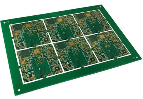
It refers to the larger substrate on which individual PCBs are arranged so that they can be fabricated and assembled. This is typically for panels or smaller boards that are designed with pre-defined dimensions, configurations and spacing for placements of the boards.
In fact, PCB standard panel sizes function as a platform where each PCB is placed together and ready for processing. Such a design strategy gives to the manufacturers the opportunity to simplify material flow, maximize the utilization of materials and increase efficiency through processing more PCBs at the same time.
In a way, standardization of PCB panels gets everyone in the electronics manufacturing supply chain on the same page, which makes it easy to work together. Through following strictly defined industry standards in terms of panel sizes and arrangements, companies can attain economies of production scale, limit costs and expenses, and maintain quality control.
Overall, PCB standard panel sizes provide a structured guideline for efficient manufacturing and assembling while saving the time and costs of several PCBs, which is key to the success and competitiveness of electronics manufacturing operations.
What are the standard printed circuit board panel sizes?
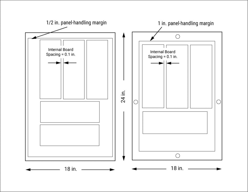
Many designers, however, base their work on the standard board dimensions, which is equally important as having designs which are aligned with the target standard panel sizes Typically, the common standard panel sizes are 18 × 24”, 18 × 12, 9 × 24, and 9 × 12 clearance around the panel border. Generally, the manufacturers recommend a clearance of ½” that goes around the periphery for handling. However, for multilayer boards, this can also be 1”.
Here are some typical PBC standard panel sizes:
1. 18″ x 24″ (457 mm x 610 mm): It is a standard panel with ½ inch of clearance for double-sided boards. Among the zigzag, divergent, and parallel configuration patterns, this is one of the most frequently used standard configurations. It takes the sizable board space necessary for putting in multiple PCBs and helps in making part orders and processing easier, as well.
2. 21″ x 24″ (533 mm x 610 mm): Another frequently used standard size, hovering a bit under 18″ x 24″, is people’s best choice to accommodate PCBs and components as to a greater extent.
3. 24″ x 26″ (610 mm x 660 mm): A bigger chip area is also the standard size commonly used to handle the greater component counts needed in larger PCB sizes.
Methods for Printed Circuit boards depanelization
Printed circuit board (PCB) panelization refers to grouping of multiple PCBs on a bigger board to minimize costs and enhance production efficiency. With this layout, many board boards can be processed and assembled simultaneously, reducing production time and cost.
The panel depanelization of a printed circuit board can be performed with several different methods, where the specific PCBs are separated from the large panel and contained after assembly.
V-Groove: V-grooves are deepened on the panel board borders as by milling or scoring. Following assembly, the PCBs can be very simply put apart along those grooves by snapping them or breaking them apart.

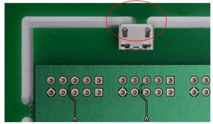
Tab Routing Process: During PCB manufacturing, manufacturers are allowed to leave these small tabs between individual boards on the panel to keep them together. These cuts (or “tabs” as they are referred to) are done after assembly of the PCBs through routing or cutting, respectively. Tabs are created along the edges of each board.
Tab routing panelization is a flexible method that can accommodate irregularly shaped PCBs and components that extend beyond the edge of the board. It is also a good way increase material utilization. Scoring is done by making grooves on each side of a panel and in between every board of a panel. Since boards are placed against each other in a panel, this removes the open space that could be used as a route path, so more boards can be placed on a panel.
Depanelization Router: A PCB depanelizer, often referred to as a depanelization router or simply PCB (Printed Circuit Board) depanelizer, is a device used to separate individual PBCs from a larger panel in the electronics industry. PCBs are usually fabricated as arrays, containing multiple PCBs connected together through tabs or small bridges named v-grooves.
Laser Cutting: One of the machine types used is the laser cutting machine, which cuts through the panel material along the determined routes, hence dividing the entire PCB.
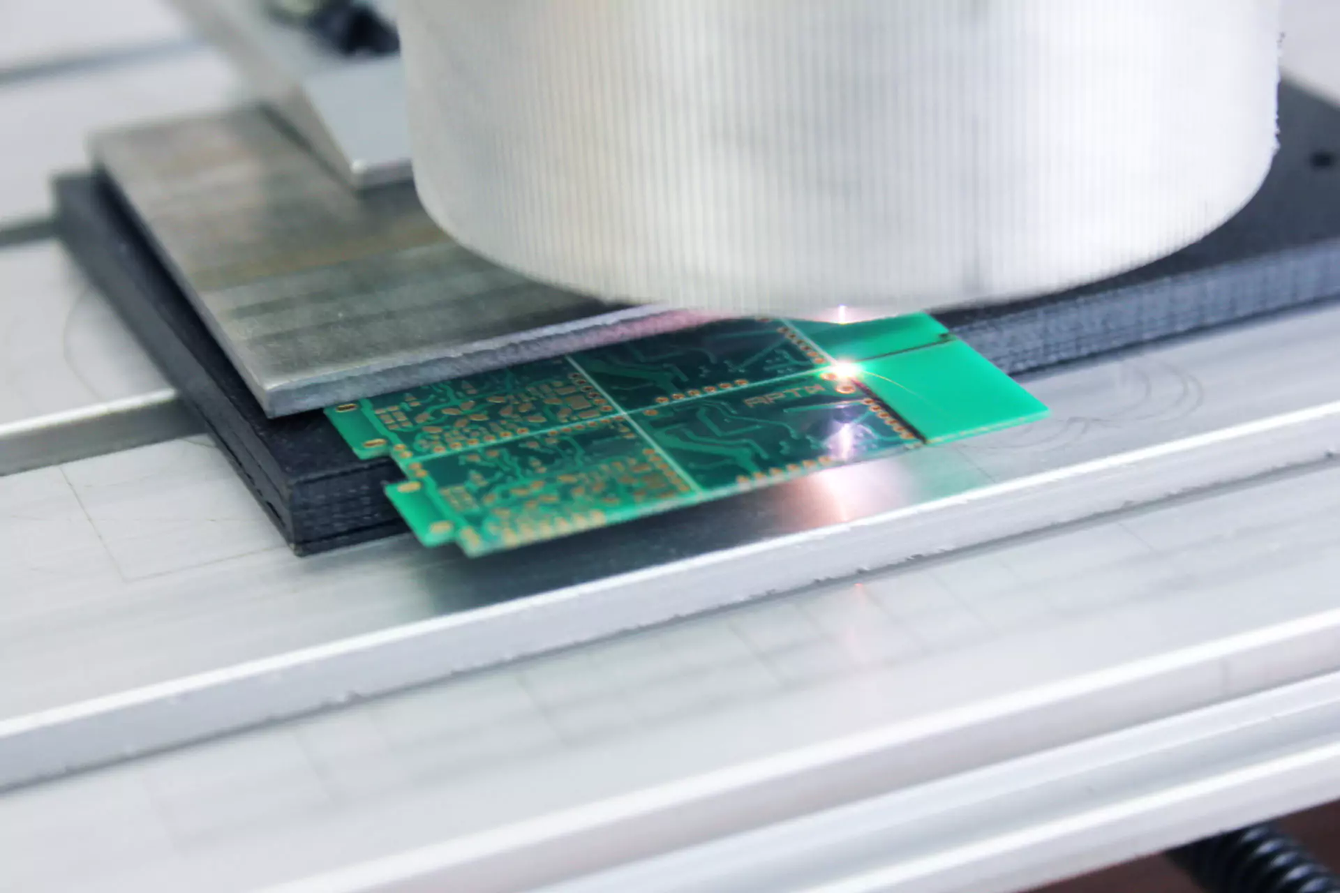
Depanelization Saw: A specially designed saw with fine edges performs cuts through the panel material as previously drawn lines at the bottom of the board split the PCBs.
The choice of depanelization procedure that must be used is influenced by different variables like the PCB design board thickness, pattern, production volume, and accuracy as well. Starting from this alternative, each technique has its own advantages and disadvantages in terms of expenses, accuracy, speed, and applicability for certain PCB models.
Why are PCB standard panel sizes important?
The PCB cores and laminations are typically available in sizes of 12 x 18 inches or 24 x 18 inches. Panel size will limit the number of boards that can be reliably produced per panel. This means standard PCB panel sizes should be considered when floor planning your board to maximize your yield of individual boards per panel. The usable sizes and PCB standard panel sizes are important for several reasons:
- Efficiency: The goal for manufacturers is to balance cost efficiency and quality control while maximizing production speeds and profits. It increases the set-up times, improves equipment optimization, and boosts outputs, resulting in the production being more effective and efficient.
- Material Utilization: Manufacturers who arrange different kinds of PCBs on a single panel/board will get an edge in terms of minimizing waste as well as saving on material costs. This is, however, slightly significant for the expensive or limited-supply materials, which will help to cut down on costs and environmental impacts.
- Cost Reduction: Standard panel sizes are the means by which computer PCB fabricators achieve economies of scale. By producing exactly the same number of PCBs with each production run, the performance at the maximum level is maintained. Such factors lead to a fixed cost distribution that reduces not only the unit cost but also the total cost.
- Quality Control: In the process of panelization, a factory can produce PCBs that are uniform in size, shape, and quality so as to avoid the use of different machines during assembly. This implies that the task of promoting the mission statement is essential, considering the risk of erroneous or defective products.
- Equipment Compatibility: Mechanical equipment and processes used in mass production are typically configured to accommodate standard panel sizes, which is a feature that promotes their intercompatibility. This results in its functioning and better utilization of equipment in production.
In conclusion, current PCB standardized panel sizes make a significant difference in the efficiency of devices, manufacturing costs, and manufacturing quality. If you need to produce a mix of different board sizes with the same thickness, you could place multiple boards onto the same panel with different arrangements to try and maximize your throughput per panel. The Sizes and Usable Areas of PCB Panels The most cost-effective PCB panels have a larger processing area. That’s why the most desirable PCB panels are 12in by 18in 16in by 18 in, 16 in by 18 in, and 18 in by 24 in. For specialized uses, panels with other dimensions are utilized.
Choosing the Right PCB Panel Sizes
Proper selection of PCB panel sizes is a vital choice for any electronics manufacturer since this will pave the way for success regarding productivity, cost, and product quality.
Standard PCB Panel Sizes
Utilizing standard PCB panel sizes can bring about various benefits when panelizing PCBs. Adherence to these standardized dimensions promotes compatibility with manufacturing equipment and processes, thereby reducing the potential for errors during production. Commonly embraced panel sizes include 18″ x 24″ and 21″ x 24″, although regional preferences and individual manufacturing facilities may introduce variations.
Tailored Panel Sizes and Considerations
If you need to produce a mix of different board size with the same thickness, you could place multiple boards onto the same panel with different arrangements to try and maximize your throughput per panel. A minor decrease in board size and rotating the boards allows two more boards to be produced per panel.
There also needs to be some space between boards on a panel to allow for manual removal or automated routing . The panel size will limit the number of boards that can be reliably produced per panel. This means standard PCB panel sizes should be considered when floor planning your board to maximize your yield per panel. While standard sizes offer convenience, there are circumstances where custom panel sizes become imperative to accommodate unique designs or specific manufacturing prerequisites. However, customization must navigate a delicate balance between optimizing material usage and ensuring manufacturability. Designers should engage in close collaboration with manufacturers to ascertain the most appropriate panel size that satisfies both design specifications and production requirements.
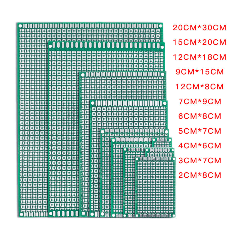
Types of PCB Assembly
Printed Circuit Boards Pcb assembly process onto panels is a process that uses many methods and techniques in electronics manufacturing.
- Single PCB Panel AssemblyUsing this technique, PCBs are either assembled individually or mounted onto a larger panel. This is a simple method of plating each component to a panel, usually with interstitial spaces available for handling or processing.
- Panelized ArraysPatterned arrays use several PCBs on one large board where the panel size is standardized. The PCBs are used in tight location on the panel, greatly increasing material use and production efficiency. In light of being assembled, the panelized array will be treated as a single unit that will then be disintegrated into separate chips.
- Step-and-Repeat PanelsRepeat pattern: step-and-repeat panels consist of panels composed of identical PCBs repeated across them. This method is suitable for high-volume production of the PCBs that are copies of one another, as the assembly process employed upon each copy of the PCB is the same. The mass production of consumer electronics and the items, which are in high demand, are usually done by the step-and-repeat panels.
- Depanelization TechniquesFollowing the assembly, we have to split either panelized arrays or step-and-repeat panels into single PCBs. Depanelization processes cover various techniques, including routing, scoring or mechanical cutting, aimed at ensuring the elements and circuitry is not damaged as the PCBs are being separated.
- Selective SolderingIn some cases, selective soldering is used to solder specific components or component areas on the panel. This enables for the attainment of high degree of accuracy in soldering process. This is vital since through-hole components and areas with thermal considerations are involved.
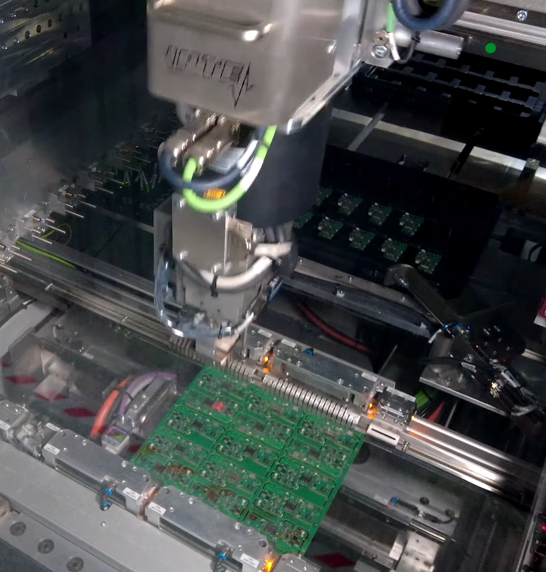
- Automated AssemblyA lot of the panel assembly processes (PAP) are being implemented using automated equipment such as pick and place machines, solder paste printers and reflow ovens. These machines can either do the placement of components exactly or the printing and reflow of solder, making efficiency and consistency in the assembly process more real.
All of the different methods of electrical panel assembly have their own advantages and disadvantages and depend on factors such as production volume, PCB complexity, and assembly requirements per complete panel. One of the important ways to do this is by selecting the best method of assembling the panels. This is the key to getting streamlined production, low costs and high quality out put for the products.
Size and location of fiducials
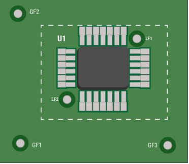
Fiducials or fiducial markers, are the reference points marked on a circuit board as a reference for automated equipment. The fiducial marks are classified into two categories:
- Global fiducial markers: These are placed on the edge of the board and help to identify the orientation of the PCB with respect to the X-Y axis.
- Local fiducial markers: These markers are placed on the outside edge of any quad-packaged SMT component.
Conclusions
In the current era where the electronics world revolves around precision, speed, and cost-effectiveness, it becomes very apparent why the use of standardized PCB sizes is a non-debatable necessity. This standardization is the core factor that enables all the elements within the production chain to operate in the most efficient and economical manner, with far-reaching and concrete advantages that leave a lasting impact within the production environment.
To begin with, standard sizes are the keys to fighting against mistakes and establishing similarity during manufacturing procedures. The PCB dimension guidelines that adhere to the frequently followed panel size standards enable the manufacturers to match these PCBs into their production lines easily without the need for new setup actions, which results in an increase in the assembly line efficiency level. Therefore, it makes the manufacturing processes smooth and decreases the chance of producing goods with defects tremendously. As a consequence, it will be satisfying to the customers, and they will undoubtedly appreciate the quality of brand products.
The process of continuous debate about standardization versus customization is undeniably inherent to the industry. While main sizes usually work, there are indeed conditions where appositive characterization is the only choice left. Nonetheless, cooperation between designers and manufacturers achieves harmony between new products and established production lines, as well as ensuring that the methods to manufacture mass-produced products are not ruined by individualized productions.
Also, the standardization of PCB sizes stimulates creativity and an ecological attitude in the process of electronics invention and making. This thus leads to the origination of related routines and instruments that are being used to enrich industry practices and give guidance on the way for a bright future. Besides a standardized size, PCB sizes are essential for the conservation of materials and the reduction of energy consumption during the production process of electronic devices, thereby minimizing waste volume as well as maximizing resource efficiency.
Overall, standard PCB sizes have a close connection to the manufacturing efficiency of the electronics industry due to different reasons. This standardization has been achieved by improving interoperability and flexibility, thereby promoting creativity and sustainability. Using standardized PCB sizes achieves production processes with ease, reduces costs, and ensures products are ready to be marketed in a shorter time. Like the apparel industry, where size standards are key components for it to run smoothly, the PCB size standard is the very force that owns this industry, therefore driving innovation, sustainability, and improvement.

