Welcome to PCB via— the main device of modern electronics. Generally overlooked, the microscopic traces are the vital arteries of printed circuit boards (PCBs) because they provide the opportunity for the smooth current to move between different layers without hesitation. The strength of PCB vias is that they are found in almost any electronic device, from smartphones to spacecraft, with which we communicate daily. Although, what exactly are PCB vias, and why are they important at all? In this article, we start off a journey in solving the puzzles of PCB Vias. We’ll reveal their significance and classify them to know the role they play in shaping the world of electronics. Whether you are an engineering student with ambitions or just a wonderer, it is now time for you to unravel the mysteries encompassing PCB vias by probing deep into the heart of circuitry.
What is a PCB via?
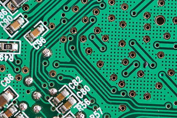
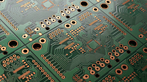
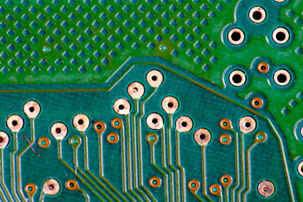
A printed circuit board (PCB) via, or via for short, is a small drilled hole that creates electrical connections among adjacent layers of a PCB. It is a plated-through hole in a PCB that you can use to route a trace from your board’s surface layer to the inner and other layers. It aids providing a conductive path for transferring electrical signals and power to be in motion between layers of PCB as well as other conductive materials; thus, printed circuits offer an opportunity for interconnections between components and traces on such layers. Vias PCBs are integral for the operation of multilayer PCBs as they allow the flow of currents and data to travel through the circuits within the PCB.
PCB Layers
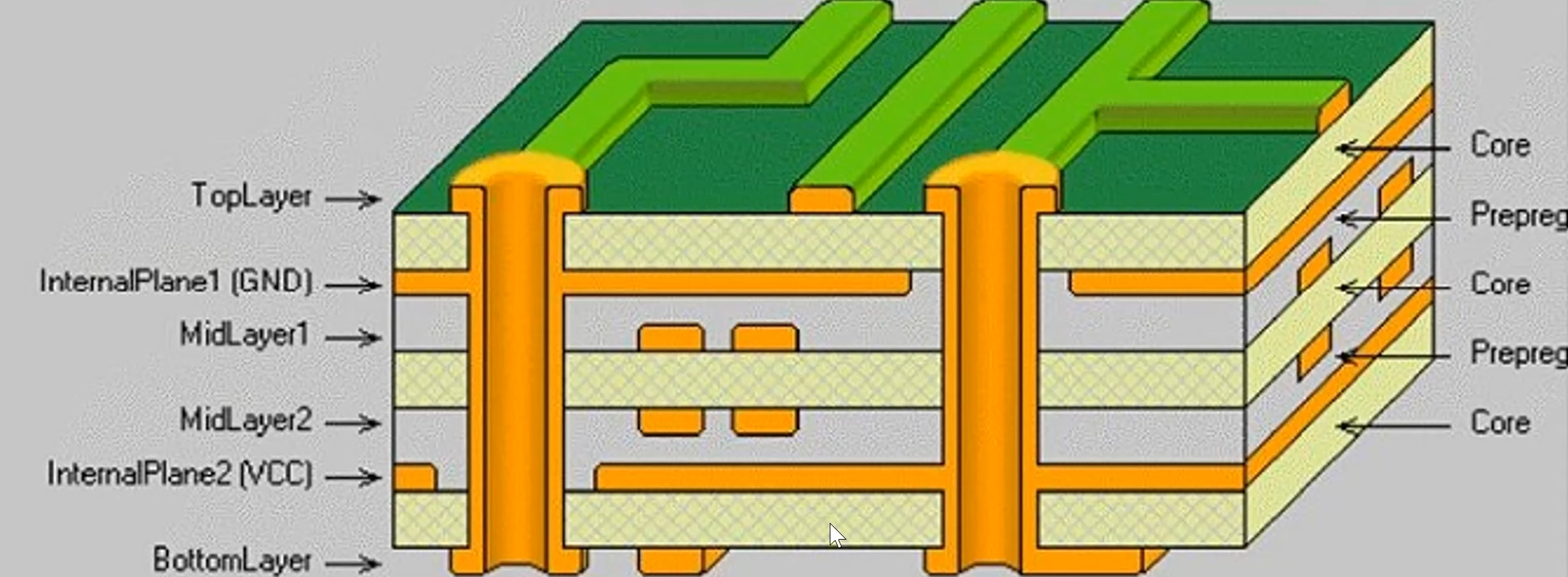
The conductive paths that are on the surface of a printed Board are commonly known as the Layers of a PCB via annular ring. Such pathways act as current carriers between different PCB Layers. As a result, signals are able to pass from one layer to another.
Since a multi-layer PCB contains vias that can traverse through all layers, laying them down side by side helps create complex signal routing. The layers of a PCB via include:
- Top Layer: The PCB’s top side is the outermost one, where components are usually mounted and soldered.
- Inner Layers: Stacked between the top and bottom surfaces in the layers. Electrical paths of different planes and components are embedded in these layers, with vias used to make the connections between different layers.
- Bottom Layer: Just like the outermost layer, here we also have metal lines and parts inside. Vias can run continuously from the top layer, through the different layers, to the bottom layer, allowing for the tying-together of all layers of the board.
The number of layers in a PCB can vary based on system of circuit and the design requirements. PCBs can be simple, having one side only with conductive conductors or they can be complex, having more than one inner layer and vias.
What are the components of a PCB via?
There are different types of vias, with different possibilities for how the vias would appear on the surface of the fabricated PCB. Although they all perform virtually the same function, they are chosen according to the particular PCB design requirements to make for a reliable PCB assembly.
Barrel:
Conductive tube filling the drilled hole Pad — connects each end of the barrel to the component, plane, or trace Antipad: clearance hole between barrel and metal layer to which it is not connected A via, sometimes called PTV or plated-through-via, should not be confused with a plated-through hole (PTH), which can also be used as holes for mechanical connection. The barrel’s strength is often affected by the aspect ratio, which is computed from the barrel’s length (L) and the hole diameter (D) and is the most crucial factor determining how the barrel performs.
Pad:
A ring, usually called a ring, is a brass annular area designed to connect both ends of tracks to components on PCB traces Siemens capabilities in driving automation and digitalization can be analyzed considering the benefits and implications of this course of action.
Antipad:
In addition, there is a dead passageway that forms an envelope, separating the rampant ring from the engulfing rings. Moreover, it is intended to provide means for guarding unwanted signal prints that could inadvertently fit into the desired plated hole.
What are the different types of PBC via?
Differences in vias take the form of via size, pad shapes, and hole diameters, which are specifically made for individual PCB needs. The main types of holes or structures are through-hole vias, blind vias, and buried vias. Another kind are skip vias, stacked vias, or staggered vias, as well as microvias, or vias in pads.
The types of vias are explored in detail below:
Through-Hole Vias:
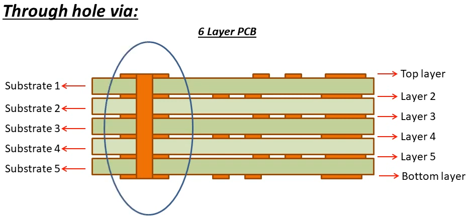
The through-hole via is the most common type of via in PCB manufacturing, which connects the inner and outer layers and passes through the entire board. Using a mechanical drill, holes are pierced from the top layer to the bottom layer and channels are established in between circuit boards through which current flows and contacts are made. These vias can be plated through-hole (PTH) or non-plated (NPTH), with PTH vias often serving as electrical connections between printed circuit board layers. However, NPTH vias are usually used for screws or connectors.
Through-holes per core: it is possible, though more expensive, to create blind or buried vias by using additional cores and lamination steps. It is also possible to backdrill and remove the plating from one side through to the desired layer, which leaves the physical hole as a through-hole but creates the electrical equivalent of a blind via.A blind via extends from one side of the outer layer (either the top or bottom layer) and connects at least one inner layer, but does not pass through the entire board.
Blind Vias:
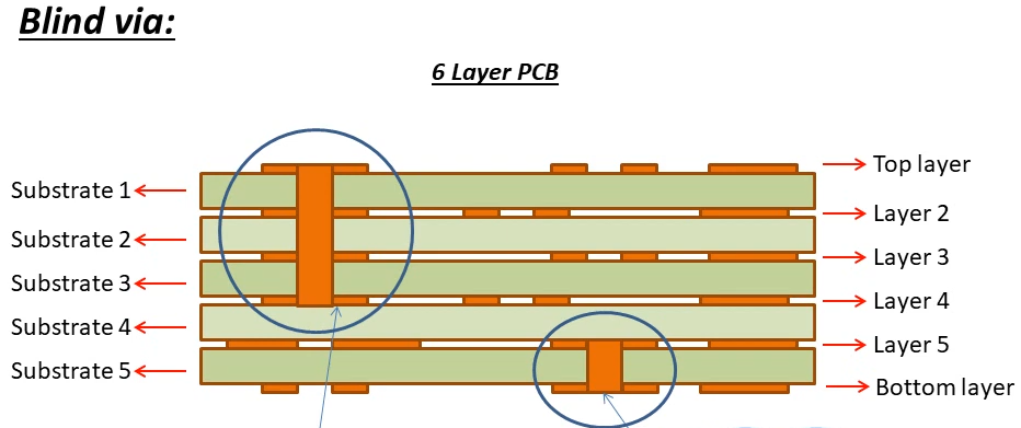
From outer layer to inner layer, blind via extends from one side of the outer layer (either the top or bottom layer) and connects at least one inner layer, but does not pass through the entire board. They can be performed from the surface and through the center of the earth, either through mechanical drilling, laser-drilling, or electroplating. Blind vias do not reach their full penetration to the board’s final layer, which is the only gap among outboard pieces.
It makes the blind vias preferred in HDI PCBs, as they give quick and accurate connectivity, which support the progress of the miniaturization of the board. Moreover, they create new connections that are not connected in one direction or lead through the adjacent place, whereas the vias occupy place.
Buried Vias in pcb design
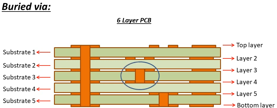
The buried via is a copper-plated hole that connects two or more internal layers of the board and is not accessible by the external layers.In printed circuit boards (PCBs), there is a type of via where the via is limited to the inner layers (From inner layer to inner layer) of the board. In contrast, it joins the interior layers of the PCB with no obvious locations on the board surface. Buried vias are generally produced as part of the ongoing PCB manufacturing process by drilling through multiple layers of the sheet and then filling the empty hole with a conducting product. This allows for a more targeted use of space on the PCB surface and makes possible to build more concentrated circuitry. Concealed holes are often found in multilayer PCBs where the space is a limited factor and the quality is a matter of importance.
Stacked Vias
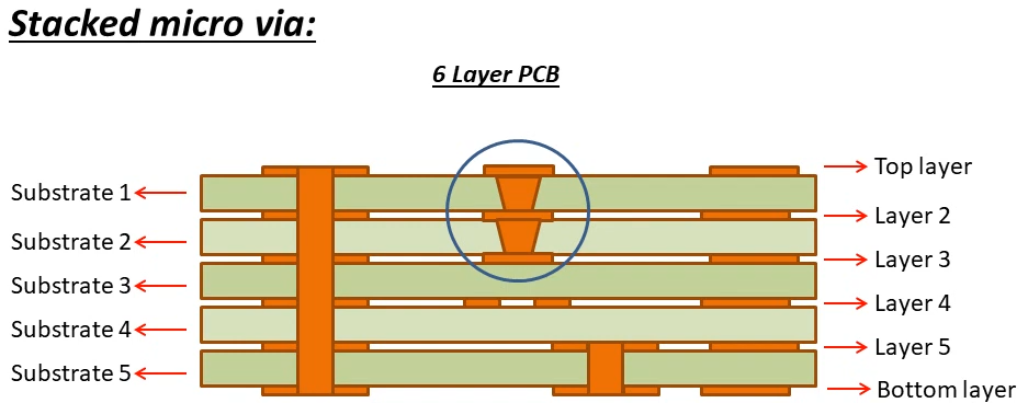
Stacked vias, also known as stacked-through vias or staggered vias, are a group of vias in printed circuit boards (PCBs) stacked vertically from top to bottom. Unlike traditional vias that are in-plane and connect only two layers, stacked vias are stacked in a vertical manner and can connect several layers. This design enables not only more routing density but also space-saving on the PCB as well. Stacked via is often implemented in HDI PCB designs where space limitation and signal integrity play a vital role. They offer a method for routing tracks between layers of a PCB, avoiding an increase in board space or increasing the layer count.
Staggered Vias
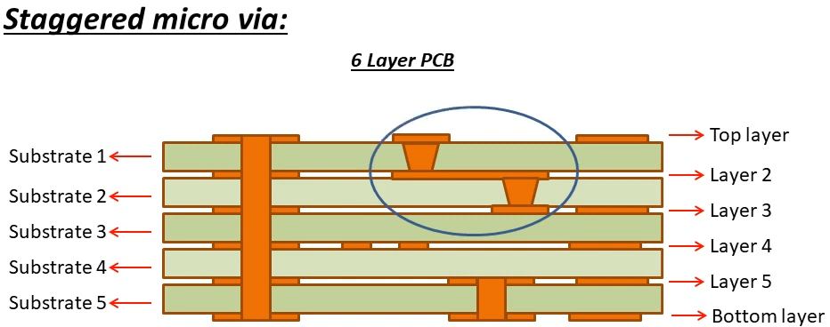
Staggered through-vias, also known as offset through-vias or overlapping through-vias, are a species of void design which is used in printed circuit boards (PCB). The outlying vias and the viatic abutting layers are staggered or offset with respect to one another. It stands for the fact that the center of the vias is not displaced, but instead, the vias are pushed in the horizontal direction of the strip.
Traditionally, vias that tie conductors together are staggered to reduce signal interference and crosstalk between adjacent vias, with this approach being particularly valuable for high-speed and high-frequency PCB designs. If the vias which are next to each other are staggered, the electromagnetic fields produced by the adjacent vias create interference with each other, and RFI is minimized.
Moreover, staggered via lowers the vibration as the layout distributes the vibration source more evenly. Hence, the possibility for a stress concentration at specific areas if there were no staggered vias is greatly reduced.
Skip Vias
Skip vias, termed as jump vias or selective vias, reveal a category of via construction utilized in printed circuit boards (PCBs). They make way for specific layers in PCBs to be skipped when a via connection is made. Skip vias instead of connecting adjacent layers are connected when required and a space of one or more layer in between is “skipped”.
Basically, skip via is a kind of Flexibility and optimization tool which helps the designers meet their specific and particular design objectives by ensuring signal integrity and routing correctly.
Microvias
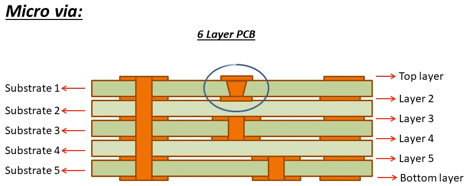
Microvias are really small-diameter vias (via is a power-delivering point at the PCB) used for high-density interconnect (HDI) designs. In most cases, they are considered to be at least 150 µm wide (or narrower), the size being defined either in accordance with the industry’s specific standards or the limitations imposed by general manufacturing technology.
Vias in Pad
Via in pad, or VIP (Via in Padding), also known as plated-over vias, is a design technique in which vias are embedded in the contact parts (solder pads) of surface components on the printed circuit board (PCB). Through-the-hole via-in pad is an archetypal design of dense PCB, which is prevalent in high-space and signal integrity-sensitive applications. When utilizing this layout, the via will sit smoothly under the component’s solder mask pad, making a straight link between the component lead and the inner tracks of another layer of the PCB.
These vias can either be standard thru-hole vias or microvias, but their position in a surface mount padmakes them unique. If a standard mechanical drill is used, the via will require extra fabrication steps to prevent solder on the pad from flowing down through the hole.
How do I make a Via on a PCB?
To create a via on a PCB, follow these general steps:To create a via on a PCB, follow these general steps:
- Design Software: Using PCB design software like Altium, Eagle, KiCad, and many other types of software, you will be ready to lay out your printed circuit board.
- Placement: Choose the point on a PCB layout route map where the via will be located. Identifying the possible positions of the components should include signal integrity, thermal management, and manufacturability.
- Select Via Type and Size: Pick the correct size and type of VIA there shall be in your design. The basic ones are insulated metal vias, which are separated into plated through-hole vias, plated through-hole vias, 3-D vias, which are buried in vias, microvias, and, of course, more. The size of the via should be in agreement with the specifications of your own design and be either a current carrying size or limited accordingly due to other space considerations.
- Place Via: Invoke the software’s operational means and then place the via on the PCB layout at the preferable position. Make sure you have the via perfectly aligned with the traces you need to connect.
- Route Traces: Through utilization of the routing tools available in the software, link the via points to the traces in the PCB layout. Make sure to interface the traces efficiently to the via so you can set the electrical flow movement to the required direction.
- Verify Design: Perform design rule checks (DRC) plus signal integrity analysis to be sure that the vias locations and routing adhere to the design rules and requirements. Perform proper adjustments to achieve the best balance between design performance and manufacturability.
- Generate Manufacturing Files: When the design is ready, create Gerber files, drill files and NC files for PCB fabrication and manufacturing. The relevant files will show the manufacturer what the PCB via type is and how to fabricate the PCB with the same type of via.
- Fabrication: Fabricate the manufacturing file for the necessary PCB components for manufacturing. The via will be drilled later during fabrication, depending on dimensions highlighted in the drill file.
- Assembly: After fabrication, a PCB is stacked up with components using the soldering method. The vias under the surface mount the components, which require special attention to be given with solder so as not to cause the solder mask to wick into the vias during assembly.
- Testing: PCB is tested to confirm all the connections are intact and the board is running smoothly as expected after the board came together.
Apply these precautions and you handle the via foiling process within the printed circuit board on a successful note, which realizes connections among various layers and components.
The Importance of Vias When Designing a PCB
Importance of Vias When Designing a PCB If you have a simple circuit board, you may not need vias. But you need vias when you are dealing with a multi-layered board, as mentioned earlier. Vias will help you establish excellent component density in multi-layered boards.
Vias appear to be small parts on a PCB (prints circuit board), but actually, they are the main elements in supporting the operation, reliability, and performance of the entire circuit board.
Here are some key reasons why vias are important in PCB design:
1. Electrical Connections:
Inlayed conductors or vias are used to accommodate the connection between different layers of multi-layer PCB. Via these layers, the tiny signals are being passed from one layer to another and consequently, the routing of tracks becomes more and more complex but the signals transmit properly via a board.
2. Signal Integrity:
The right locations of the Vias act as a medium to safeguard signal integrity by reducing signal loss, impedance inconsistencies and electromagnetic interference (EMI). With the low impedance pathways offered by them, vias lastly help to keep the signal quality intact.
3. Thermal Management:
Vias are also the source of heat management in PCBs, especially in structures of high-power components or in times when heat dispersion requires attention. There are multiple advantages to thermal vias over other materials for taking away heat from hot locations of circuit boards. On the basis of this reason, thermal vias improve overall gadget reliability and prevent overheating.
4. Component Placement:
Traces can be routed and component placement can be achieved by the strategic placement of vias in between circuit layers. They enable designers to have trace optimizations and component placement, which is to make sure the signal path lengths are minimized and that no traces crosstalk.
5. Mechanical Support:
Via can be used to attain extra rigidity as it adds more support for the components or specific points used as a mount. Vias made by through-hole tend to be of a pattern that provides the board with mechanical strength and protects against bending or sagging.
6. Layer Transition:
The Vias are the components that guarantee a functional changeover between the various layers in the multilayer PCB. They are responsible for the conduction of these traces that interconnect layers and save much-needed board space by utilizing the small form factor.
7. Cost and Space Optimization:
Strategic placement of the components is one of the many solutions to decrease fabrication costs and provide a more efficient use of board space. By process refinement, building the structure in stages or dropping multiple layers down, the designers are optimizing the area, and the size of the appliance becomes the reason for the decrease in cost.
In conclusion, as vias perform numerous functions in the PCB mechanism, ranging from easing electrical connections to managing thermal issues and providing the best space utilization, these are imperative in the design and manufacturing of electronic products. A concern with vias implementation is whether PCBs are able to perform well, endure the test of time and be eco-effective. Thus, perfecting the insertion of vias is crucial for final PCB performance, quality and efficiency.
Conclusion
In the complicated electronic world of PCB design, the inconspicuous vias represents the hidden hero on our circuit boards that link layers, manage signals, and strengthen structural board integrity. “Into the Core: “Understanding the Fine Print of PCB Vias” uncovers the intricate workings of these small components, debunking the myth of their seemingly insignificant presence in the world of electronics.
role of vias in layering electric connections, protecting signal integrity and dealing with thermal problems can not be underestimated when the design is completed, based on values of these points. In this regard, their location of choice not only guarantees the smoothest movement within the factory but also allows them to make the best use of available space and keep the manufacturing cost at a minimum.
Alongside their technical capacities, throughs combine analytical thinking and artistic prowess, where attention to detail and imaginative skills unite to attain high-level effectiveness and resilience. ICs wouldn’t function as well without PCB vias, which is at heart the epitome of creative innovation.
Eventually, the study of connection point vias will give knowledge of PCB layout more depth and will facilitate the introduction of new technological inventions. As we voyage further into the borderless exploration of the electronic world, the fact that these small but significant elements, which are at the center of each electronic gadget, are never ignored should always remain in our minds.