Welcome to the world of electronics manufacturing, where precision and performance dictate right down to the thickness of a Printed Circuit Board (PCB). Thickness is a critical dimension. Here we are, trekking around the fragile ecosystem of the balance between the board thickness and performance. The article below will take you through the detailed world of PCB thickness standards, unwinding the knotty areas and showing you the way to the best overall circuit board thickness for your electronic interests. Follow us deep into the secrets for a balance of the best improvement in electronics with PCB thickness standards.
Basics of PCB
Printed circuit board (PCB) is thin layered board, usually composed of fiberglass or composite epoxy laminates. The main role of a PCB is to act as the mechanical substrate for the mounting of a system’s components. It also offers the essential enabling channels through which electrical impulses are passed from one of these components to the other organization. These are usually created as lines of a copper foil and embedded in the surface of the PCB In order to make a trace.
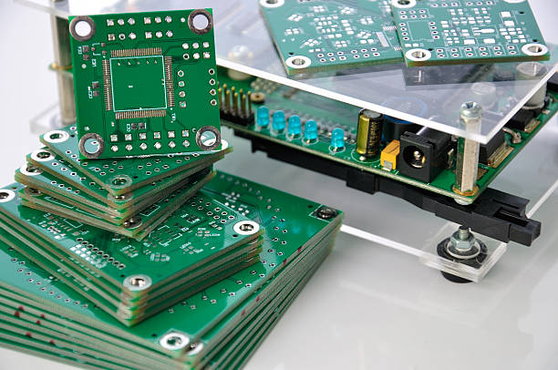
The design of a PCB involves a number of essential features, such as number and configuration of layers, placement of components and where they will be held, and the route of signal traces. But, there is another dimension that is usually ignored, but it is equally crucial, and that is the thickness of printed circuit boards.
Importance of PCB in Electronics
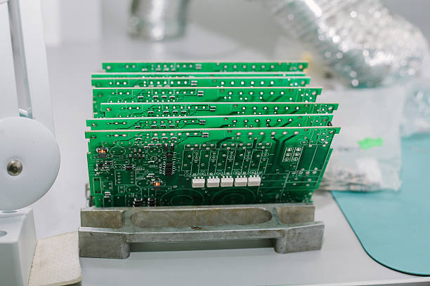
PCBs play a very important role in today’s various electronic devices and gadgets. In simple terms it acts as a medium through which various electronic components like resistors, capacitors and integrated circuits can be mounted and connected. PCBs save the time and trouble that would be required for the connection of these components manually with the use of unreliable and complex wiring arrangements.
- They possess a high degree of miniaturization that allows the production of compact and lightweight electronic devices.
- They safeguard standardization in production and thus provide consistent quality for their products.
- They facilitate problem diagnosis and fixing: The layout of the components and connectors is defined and consistent.
Practical applications of these advantages are determined by the PCB thickness. It directly affects the board structural integrity and thermo-mechanical properties as well as its manufacturability. As such, a correct specification and understanding of PCB thickness is of paramount importance in PCB design and its manufacturing processes.
What is Standard PCB Thickness?
The thickness of a PCB (Printed Circuit Board) is an important characteristic of printed circuit boards that is related to the mechanical stability and thermal performance of a PCB and also, to possible end applications. There are various thicknesses of PCB core thickness that can be used to achieve certain specifications; at the same time there are standards thicknesses that can be used in PCB fabrication. Attached is a working table that contains information on the standard thickness of the PCB and the factors that may affect the thickness selection.
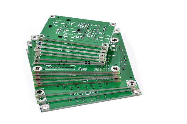
Common Standard PCB Thicknesses”
- 1. 6 mm (0. 063 inches):
- Most Common Thickness: It is the preferred thickness and is used in almost every PCB application solution from consumer electronics to industrial equipment.
- Benefits: Promotes strength and durability as well as the price. Its excessive thickness is necessary for mechanical strength and support of the components.
2. 1. 2 mm (0. 047 inches):2. 1. 2 mm (0. 047 inches):
- Use Cases: used for the small devices, where the space is minimal and some degree of rigidity of the device is needed.
3. 0. 8 mm (0. 031 inches):3. 0. 8 mm (0. 031 inches):
- Use Cases: Ideal for small and light use cases like in personal mobile phones, smart watches & similar wearable gadgets or nanodevices. It is thicker than the thinner boards and is more flexible.
4. 0. 6 mm (0. 024 inches):4. 0. 6 mm (0. 024 inches):
- Use Cases: Flexible substrate or semi-flexible can be applied in various PCB designs to obtain medium flexibility and mechanical stability.
5. 0. 4 mm (0. 016 inches):5. 0. 4 mm (0. 016 inches):
- Use Cases: Common in those highly compact devices where flexible materials are necessary rather than the rigid ones. Typical for high density requirements and flex-PCB.
6. 2. 0 mm (0. 079 inches) and Above:6. 2. 0 mm (0. 079 inches) and Above:
- Use Cases: Used in applications that require additional strength and back up like high-current mains, heavy commercial electronics and some automotive applications.
Factors Influencing PCB Thickness
Printed Circuit Board commonly known as PCB is a very complicated structure which is used in many electronic devices, gadgets and machinery’s; here thickness of the circuit board thickness, is something which decides its capacity, life and usability level of the product for which it is being used. The following are the factors that play a vital role in this important aspect, each of which contributes to the board’s qualities and potential in a complex manner:
Substrate Thickness
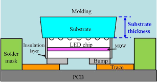
The substrate, normally with FR4 material, polyimide, or CEM, is at the base of the PCB as the mechanical support anti-stress layer. Decisions of the material used in the substrate and its thickness determine the PCB’s capabilities to withstand thermal stress, mechanical shock as well as harsh conditions.
Higher trace thickness (around 3. 2mm) is useful in more stressed environment applications; this is for instance used in automotive industry. Thinner substrates with trace thickness (0. 8 mm to 1. These include low-profile terminals (≦ 0 mm) are ideal in small form factor devices such as; smart phones, wearable devices and more.
Prepreg Thickness

Prepreg is a dielectric material that accompany the preparation of PCBs to serve as the insulative and bonding medium between two layers thicker boards for instance between two cores or between a core and copper foil. In multilayer PCBs, it is critical to stop the short circuit and contributes to the stability signal integrity of inner layers of the circuit board.
Made from fiberglass pre-impregnated with resin (like epoxy or partially cured polyimides), prepreg types vary by resin content: The three types of epoxy resin available are: high resin (HR), medium resin (MR), and standard resin (SR), and as the resin numbers increase, the thickness of the epoxy resin increases additionally; the cost of the epoxy resin also increases.
In the production of PCB, the materials referred to as prepreg are placed and adhered between copper foil layers, followed by heating and pressing to create laminates that play a vital role in holding and also protecting the copper foil layers together of PCB. Of the common types discussed, preg thickness influences impedance and dielectric characteristics and copper thickness ranges from 0. 0508 mm), pp-1080 (0. 0762 mm), pp-2113 (0. That produced pp-1016 (1016 mm), pp-2211 (2212 mm), and pp-2116 (0.
PCB Copper Thickness
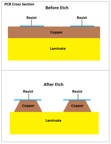
In the production, PCB copper thickness is described in terms of standard known as “ounces per square foot”. The most common form is a standard size of 1 oz which is 0. Its. copper thickness has ranged between 0. 0348 mm (1. 37 mils) and 0.05mm (2 mils). Thus, copper thickness influences the production thickness and the electrical current that can be carried by the PCB. When the boards mandate impedance control, the amount trace copper thickness, width and copper weight are significant more. Some of the considerations in defining copper thickness include; the copper weight, compatibility of the PCB for use with certain components, and the kind of connectors used.
Center layers, interior and external layers, have different core thickness according to the construction mode, while copper weight and core thickness are interchangeable. For circuits that demand the high value of current, more copper is incorporated in the manufacturing process though this is a cumbersome process.
Multi-Layer PCB Thickness
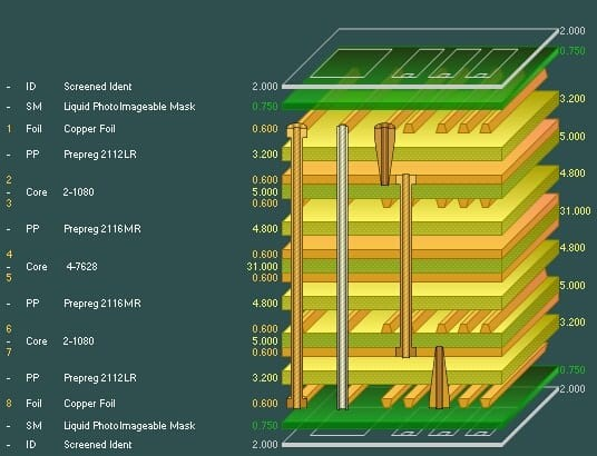
A multilayer PCB has been defined as one that has more than two layers where each layer has conductor material such as copper for the routing of circuits and the layers are well separated to avoid short circuiting by an insulating layer. Extra layers and board thickness can enable more intricate layouts and Multi-layer routing and grounds planes, leading to greater PCB thickness because of the added third copper layer and non-copper layers, known as prepreg.
These designs are very crucial in the fields of application in other complicated electronics that need the ability to interconnect the circuits tightly together, better signal transmission, and less interferences from electromagnetic forces. However, it adds more layers thicker copper, which makes production a little expensive since the pcb trace thickness two copper layers is thicker than in the previous layers, though not suitable for all applications. The number of circuits that can be accommodated, the space that is available on the circuit board and the cost are some of the factors that will determine the complexity of the circuits that designers are going to incorporate in their designs.
Solder Mask Thickness
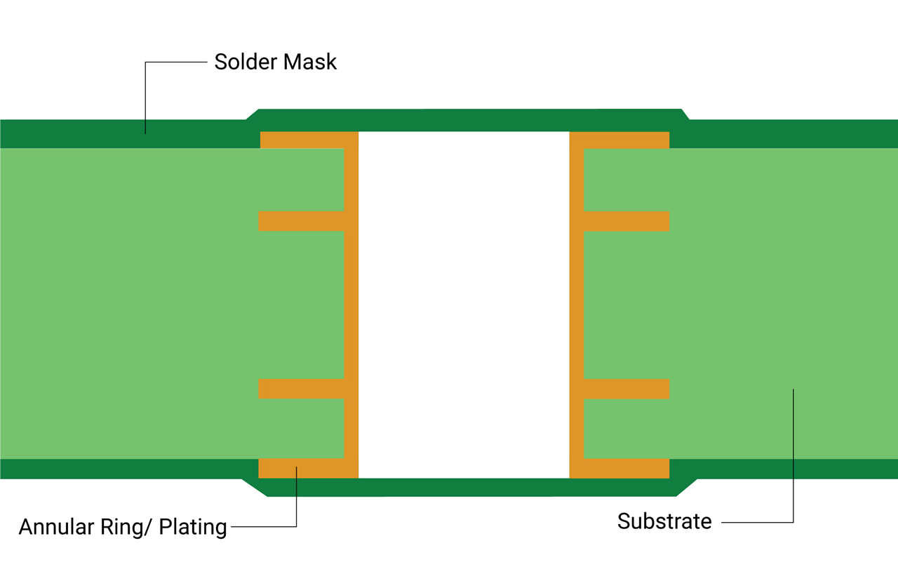
The solder mask for a PCB is a layer of material that is put over the copper traces of the board to avoid occurrence of solder bridges at the time of assembly and to avoid the copper traces from being affected by oxidation. Standard thickness of the solder mask varies between o. 05 mm to 0. Thickness is 1 mm (or between 2 and 4 mils). This thickness helps to get the best insulation for the copper traces used and also makes it easy to solder during the assembly phase. Solder mask outer layers, with more thickness are beneficial in terms of protection for the written matter, but may pose a certain challenge in the layer registration/alignment of solder mask thickness in the workflow for ensuing assembly.
Importance of PCB Thickness standard
Overall Board thickness need to be standardized for compatibility, mechanical integrity, high thermal and electrical conductivity,,, electrical characteristics, ease of production, and standardization with various international standards. This guarantees the correct positioning or alignment of the parts, minimizes warping, contributes to management of thermal expansion, offers uniform electrical characteristics, aids in assembly, and complies with regulatory standards, improving functionality, dependability, and affordability of electronics.
Choosing the Right PCB Thickness
Choosing the right PCB thickness depends on several factors:
- Mechanical Requirements: Think also about mechanical stability required by the system in your particular application. There exist thin PCBs but the ones that are thicker are more rigid, they are ideal for use in environments where either the environment or the components being used are rugged. Thinner PCBs consume less surface space than their thicker counterparts and are lighter which makes them suitable for small electrical gadgets or even for use in flexible equipment to a certain extent.
- Electrical Performance: PCB thickness has an influence on the electrical parameters of the unit, such as impedance, as well as signal integrity. Increased widths of PCBs may minimize signal attenuation and cross talk but worsen parasitic capacitance. The downside with using thinner PCBs is that they may prove a challenge to design well in matters to do with impedance especially in high frequencies.
- Heat Dissipation: The larger size PCBs are also known to have a better heat dissipation capacity because of their greater thermal inertia. Think about the thermal peripherals of a particular element and the question of whether extra cooling measures are needed.
- Manufacturing Constraints: In general, laser direct imaging is capable of handling both thick and thin copper foils; however, consult with your PCB manufacturer for more information and the specific thickness tolerance that they recommend or use. Depending on the organization’s aimed at, thicknesses might have limitations or involve costs that are hard to sustain.
- Cost: Higher levels of wiring density generally translates to higher prices because of the following reasons: The usage of thicker material adds to the costs of fabrication The fabrication process for thicker material takes more time than thinner ones. Cost can also be a constraint when selecting an application package consider it in light of the application requirements.
- Industry Standards: There are some industries or specific applications that require specific thickness of PCB for its use. As applicable, make sure there is a response to all the standards discussed within this template if any of them apply to the project.
In conclusion, the appropriate board thickness is relative to a wide range of applications both mechanical and electrical and depends on manufacturing cost raw materials, thermal control, and standards.
PCB Thickness and Manufacturing Process
Thus, the thickness of a PCB is not only a crucial characteristic of an electronic device in terms of signal quality, integrity and quality of performance but also has a huge influence on the manufacturing process. Using materials of different thickness than standard creates new difficulties and complications in the PCB manufacturing process to deliver a final product that is both effective and efficient.
- Drill Holes: A major concern when dealing with thin PCBs especially those of non-standard thickness is how to drill through hole components and vias. Thicker PCBs means the need to use longer drill bits, and this means taking more time to drill a certain number of holes thus making the manufacturing process costly and time-consuming. However, working with thicker PCBs also poses several challenges in terms of hole drilling and drill bit breakage and precise positioning of the holes.
- Lamination Complexity: One of the issues that arise in the case of manufacturing PCBs with non-standard thicknesses is the complexities involved in the laminating stage. To form a complete and compact board, there are various stages that are involved in the lamination process whereby copper and insulating material layers are placed on top of each other and then exposed to heat and pressure. Thicker multilayers PCBs may take more pressure and longer time for laminating in order for the different layers to bond well. This also leads to a possibility of having defects like delamination and warping affecting the structural stability of the board.
- Etching: It is essential to understand that the thickness of the PCB can influence the etching process that is commonly utilized to generate the conductive paths on the board. Thicker PCBs, particularly those with thicker copper foils, might take longer to etch and might need stronger chemicals for the selective removal of copper. This can lead to under-etching or overetching that may affect the sharpness of the printed circuits and hence the general quality of the board.
- Assembly: The board thickness needs more energy to apply and extended periods of soldering to make good solder joints. This heightened exposure to heat increases the experimental thermal impact, which may damage the components assembled on the board and compromise the PCB itself. In PCB Assembly, the concern lies in maintaining enough heat for soldering but at the same time avoiding thermal destruction.
- Depanelization Method: PCB thickness is also a factor in determining the method that is used in depanelization, which is the process of severing individual PCBs from a panel after production. Thicker PCBs might need better depanelizing techniques like routing, sawing or cutting as compared to thinner PCBs which can be easily depaneled by scoring or laser cutting. However, the selected depanelization technique must not require excessive cutting through the PCB thickness to avoid imposing a lot of stress on the boards in the process of carrying out the depanelization process.
Therefore it is clear to see that the thickness of a PCB is important in the manufacturing process and designers have to be sure that the thickness they chose right for the manufacture of the board. When the thickness of the PCBs does not conform to industry standards, designers can evaluate these difficulties and consider options for thin boards or thicker board that accomplish the desired performance while minimizing fabrication issues.
The Importance of PCB Thickness in Heat Dissipation
Another important factor that is also influenced by PCB thickness is the rate at which heat and coolness are exchanged within an electronic device. Here’s why:
- Thermal Conductivity: Thicker PCBs essentially are known to have higher thermal conductivity as they contain more material in volume. It lets them effectively carry the heat away from the heat-producing parts such as a CPU or power transistors and spread the heat over the entire board.
- Heat Spreading: Thicker PCBs on the other hand are good heat spreaders, and the heat generated from the components is evenly dissipated on the surface of the board. This helps avoid localized thermal hot areas and leads to a more uniform heat dissipation meaning that the chances of having some component(s) get too hot are greatly mitigated.
- Thermal Mass: Increased core thickness in the PCB results in a product having a greater capacity for thermal conductivity and storage. This helps to regulate temperatures inside the device by providing a buffer to abrupt temperature changes, and in turn preventing the rapid temperature changes, which can negatively impact the proper operation or lifespan of a particular device.
- Mounting Heat Sinks: Thicker PCBs are more leeward to mount the heat spreader or other thermal solutions. Heat sinks can be mounted firmly so that heat transfer from the components to the heat sink and finally to the environment can be effectively done.
- Overall Device Temperature: In this case, the thickness of the PCB can control the rate at which the heat will be dissipated and therefore the total temperature of the electronic device. Lower operating temperatures will not only increase the durability of the components but also make the device more efficient.
Thus, it has been inferred that thickness of PCB is important for heat dissipation in case of end products relating to electronics. More discreet layers also provide enhanced thermal, managing heat dissipation, heat spreading, thermal inertia, and compatibility with thermal schemes, leading to lower temperatures, better device performance, and durability.
Conclusions
In the process of electronic design, it is very crucial to achieve the right compromise where PCB thickness is a factor. As discussed earlier, the thickness of the PCB impacts heat dissipation, an aspect that is essential in determining the functionality and durability of vehicles. Thicker PCBs have the benefits associated processing thicker copper with high thermal conductivity and conduction, heat dissipation, and compatibility with some thermal management technologies but the PCB manufacturing increase in difficulty, cost, and compatibility issue with existing components and covering.
When dealing with different PCB thickness, there are several essential parameters that need to be taken into consideration, including mechanical properties, electrical characteristics, thermal management issues, manufacturability aspects, and conformity to the standards used in electronics manufacturing. These aspects should be considered by designers in order to achieve the best results of performance, reliability and cost of the electronic designs.
In conclusion, it is possible to determine the best thickness of the PCB depending on the needs of the specific application, but with a little challenge due to factors such as fabrication costs. Therefore, by considering such factors as PCB thickness when it comes to component layout, designers can create circuits that dissipate heat well and in the process improve the reliability and performance of electronics products.

