With the increasing demand for high standard electronic equipment, no doubt the reliability and efficiency of those printed circuit boards (PCBs) are more pivotal. The role of X–ray inspection devices in the PCB assembly process cannot be overstated, since there is no other inspection tool that can match their image visualization of the solder joint integrity and component placement.
The guide describes the incorporation the x-ray inspection in the PCB assembly. In particular, the paper identifies the principles that will be applied, the changes that will be made, and some good practices among them.
What is X-ray Inspection Technology?

This innovative technology is considered a harmless probe method. It allows inspecting of the inner parts of the PCBs not only without damaging the boards, but also visualizing them.
In simple expressions, these devices dissolve substances and rapidly takes pictures of their interior structures. Making prototyping display boards with X-ray inspection provides a good approach for uncovering faults that were neglected using microscope viewing techniques. There’s a bizarre twist to x-rays. They become dated and then they highlight the dark spots and signals.
How does X-ray inspection work?

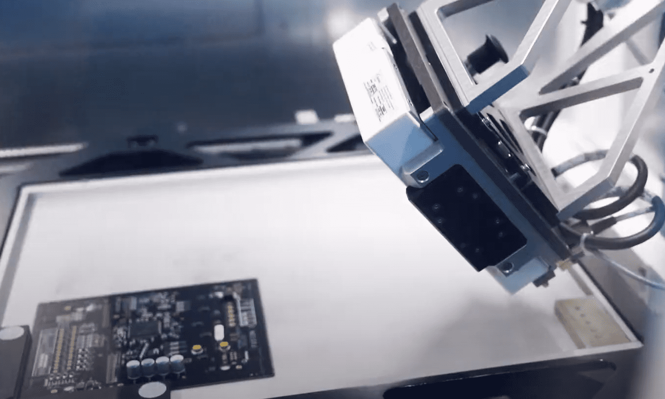
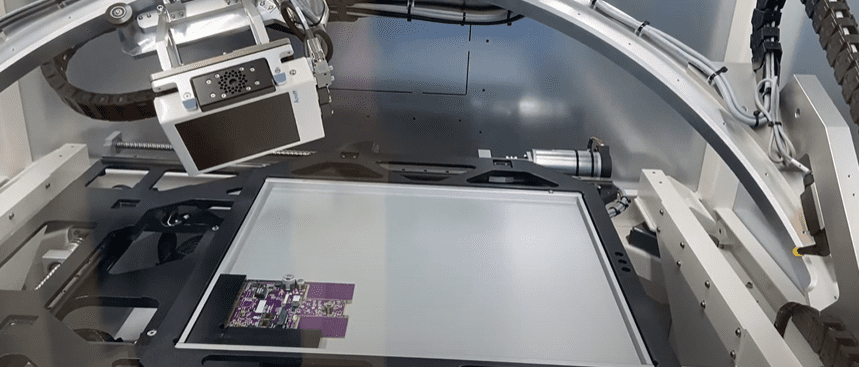
To better understand how X-ray inspection works,. All x-ray inspection devices are made up of the following basic features:
X-ray Tube: The first step of the process is the emission of a strong and sharp X-rays from the X-ray tube. This is an x-ray tube where the x-ray photons are generated.
Penetration and Absorption: While these X-rays pass through the PCB, they encounter many different substances in the circuit board that, to varying degrees, absorb them. In the dense material like in metal solder joint, more X-rays are absorbed and in less dense materials.
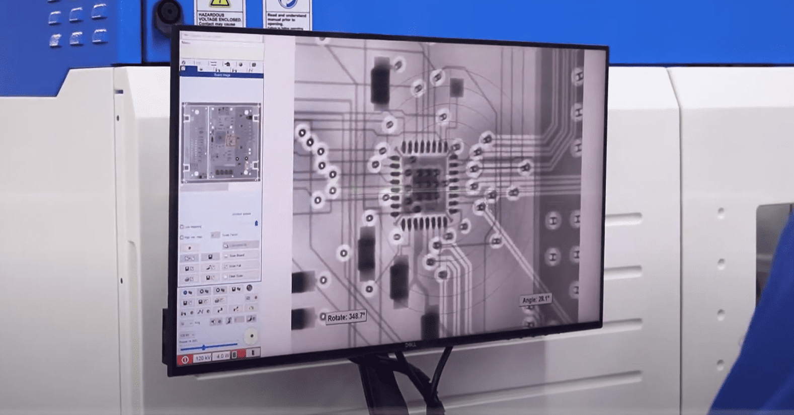
Detector: The other side of the PCB is where the detector is located, which has captured the X-rays that have passed through the board. The detector transforms the X-rays into an image; thus, a detailed map of the inner structure of the PCB is formed into a ray image.
Image Processing: The captured image is processed and analyzed using advanced software. This program improves the image, focuses on the defects, and gives a complete analysis of the circuit board’s internal structure.
Why is X-ray inspection important for PCBs?
PCB X-ray inspection plays a significant role in PCBs because of the following reasons:
X-ray inspection is vital for detecting defects in PCBs, including solder voids, solder bridges, solder voids, component placement issues, and internal layer defects, ensuring quality and reliability.
X-ray inspection aids manufacturers in meeting stringent industry standards, ensuring compliance with regulations set by organizations like IPC.
Benefits of X-ray Inspection in PCB Manufacturing
A. NON-DESTRUCTIVE TESTING
X-ray machine does not harm the PCB; hence, it can be used again and further tests can be conducted.
B. HIGH ACCURACY
It allows for a close view of internal structures and defects, thus making defect detection very precise.
C. ENHANCED QUALITY CONTROL
This method helps in maintaining high standards by pointing out defects that are not seen through other inspection methods.
D. Cost-Effective
Through the detection of defects at the initial stage of the manufacturing process, X-ray inspection lowers the expenses connected to the rework and the scrap.
E. Comprehensive Analysis
It gives a comprehensive report of both the external and internal aspects, hence making quality control an absolute guarantee.
High-Resolution Imaging

Today, the X-ray inspection systems are equipped with high-resolution imaging technology, which enables the complex analysis of the micro-scale features. These advancements have been the reason why manufacturers can now find even the tiniest of defects with the highest accuracy.
3D X-ray Inspection Technology
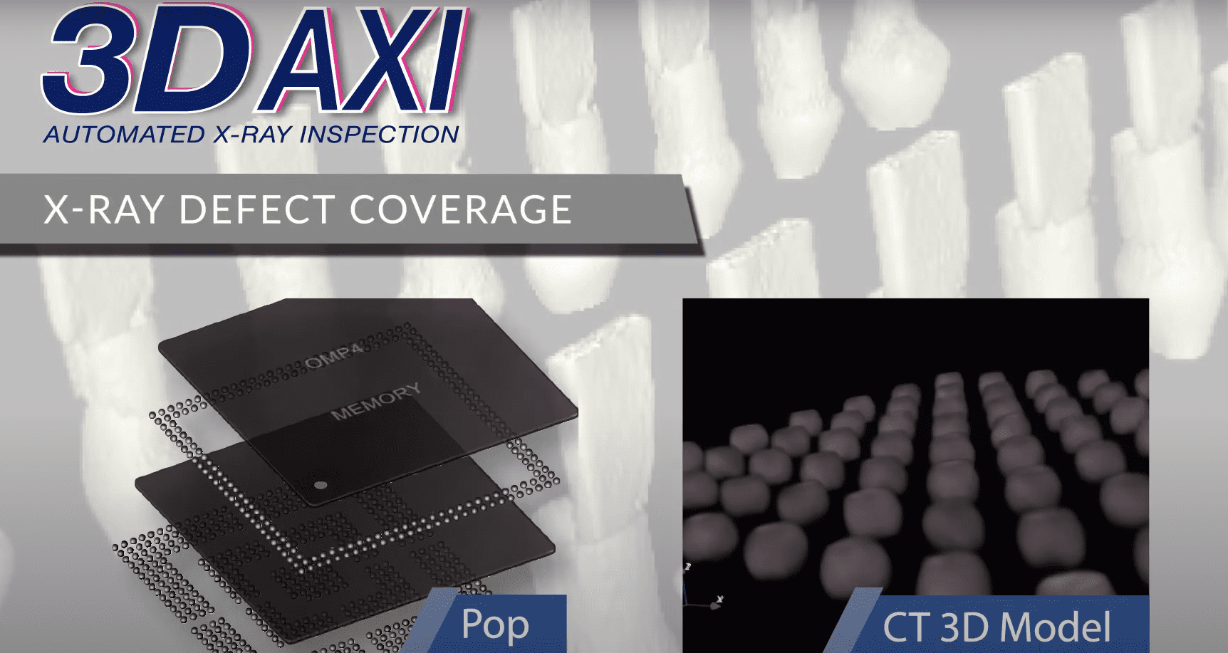
The three-dimensional (3D) X-ray inspection technology has transformed PCB inspection by providing volumetric analysis. This enables a better assessment and sampling inspection of solder joints and component placements, which, in turn, increases the detection accuracy of defects.
Automated X-ray Inspection (AXI)

AI and software algorithms are utilized in the automated X-ray Inspection (AXI) system to aid in the automatic detection of defects. AXI improves inspection efficiency and consistency, diminishing human error and quickening the inspection process.
Inline X-ray Inspection
Inline X-ray inspection systems are woven into the production line, thus permitting real-time monitoring and immediate feedback. Thus, this enables quick detection and resolution of product defects, thus increasing production yield and decreasing the cost of rework.
X-ray Inspection vs. Traditional inspection System
Choosing between X-ray and traditional inspection methods depends on the specific requirements of the PCB manufacturing process. For basic, low-cost inspections, traditional methods like visual inspection and AOI are suitable. However, for high-reliability applications and complex assemblies, X-ray inspection system provides unmatched capabilities in detecting hidden defects and ensuring the highest quality standards.
Best Practices for Implementing X-ray Inspection
- SELECTING THE RIGHT SYSTEM
The right X-ray inspection system to be chosen depends on several factors, such as the complexity of the PCBs, the types of defects that are to be detected and the production volume.
The resolution, imaging capabilities, and automation features of the system are the aspects that must be taken into consideration.
- OPERATOR TRAINING AND EXPERIENCE
Even with the help of modern automated systems, the expertise of the operators is still important for analyzing X-ray images and understanding the meaning of the detected defects. Regular training and certification programs for the operators can result in the effective utilization of X-ray inspection technology.
- REGULAR CALIBRATION AND MAINTENANCE
The accuracy and reliability of X-ray inspection systems are maintained. Thus, the whole x ray inspection equipment is always in the best possible state, which is the main reason for the uniform and high-class results.
Future Trends and Innovations
These are the feature trends and Innovations
Enhanced AI and Machine Learning Algorithms
The next stage of X-ray inspection technology will be the further development of AI and machine learning algorithms. Thus, the breakthroughs in this field will even more enhance defect detection accuracy, decrease the number of false positives, and make it possible for predictive maintenance.
Miniaturization and Portability
As electronics are being miniaturized, there is a constant demand for X-ray inspection systems that are portable and compact. In the future, innovations will probably focus on the development of lightweight and portable systems that can be quickly installed in different production environments.
Integration with Industry 4. 0
X-ray inspection technology is projected to be the key factor in Industry 4.0 revolution, with the possibility of having the devices integrated into the smart manufacturing systems. This with x ray devices will allow smooth data transfer, live monitoring, and the latest analyses, which will be the reasons for further improvements in PCB manufacturing processes.
Conclusion
X-ray inspection technology is a vital instrument in the PCB assembly process, giving a deep understanding of the quality and reliability of electronic assemblies. As the technology keeps on improving, it will definitely come with even higher accuracy, efficiency, and integration with the most up-to-date manufacturing systems.
The PCB manufacturers will be able to stay up-to-date with these innovations, and by applying the best practices, they will be able to produce high-quality, reliable PCBs that meet the requirements of today’s electronics market.

