Discover the mysterious ways to achieve PCB assembly by studying our eclectic trade and guidelines. Ranging from soldering basics or solder paste printing to last-mile component placement tips, our guide equips even beginners with critical tools for enhancing their projects and for experienced professionals as well. Plunge into the intriguing dimension of electronic design and manufacturing and find components to build a prototype for sure network quality for the sake of your projects through stability and accuracy.
What is PCB assembly?
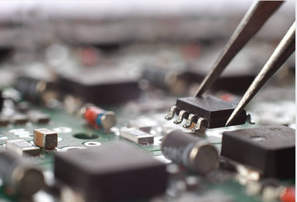
PCB assembly (PCBA) is the process of mounting electronic components on a PCB surface to make a fully operative electronic device. These parts, which are resistors, capacitors, and integrated circuits, as well as connectors, are picked and mounted onto the PCB in accordance with the design of the circuit. After it attach components, they are welded to the PCB using techniques like wave soldering, reflow soldering, or manual soldering in order to form electrical interconnections. After the assembly process of the circuit is done, it undergoes final inspection to check whether all the components of the electricity system have been placed correctly and soldered together properly. Further, these steps of the functional test and in-circuit test conduction are carried out in order to verify the functionality and performances. PCB assembly services could also be tested for conformal coating or encapsulation, which will protect the assembly labor from environmental factors. PCBA services plays a significant role in guaranteeing that electronic products and gadgets match up with quality specifications in their functioning as well as in producing devices that are durable and reliable for the intended application throughout the entire process.
What are the types of PCB assemblies?
These are the types of printed circuit board
Through-Hole Assembly (THA)
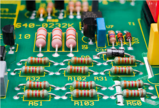
The Through-Hole Assembly (THA) is a technique in electronic circuit board mounting process in which the components’ leads or pins are inserted through the holes drilled into the board for the components to stand upright on the assembled boards. Unlike SMT assembly, which transfers components directly onto the PCB board surface, THA goes through the underside of the board to solder component leads to their respective pads on the opposite side. The THA has been a traditional approach for multiple reasons, including the requirement of stronger connections or in the manufacture of low-cost and volume assembly. Parts were designed and manufactured with the THA due to its benefits over other assembly technologies Nevertheless, THA does retain significance where misplaced components that are meant for surface mounting are unsuitable, such as those that require more strength for mechanical purposes, and continuation with THA remains popular in aerospace and automotive companies due to their resilience and ease of inspection.
Surface Mount Technology (SMT)
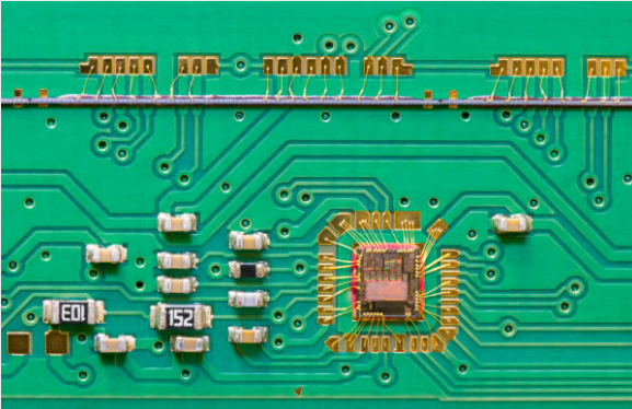
Nowadays, Surface Mount Technology (SMT) assembly is usually used for electronic circuit board assembly, whereas in through-hole assembly (THA), holes in the circuit board are previously drilled and components are soldered onto the circuit boards. In surface-mount technology, components are fastened to the state-of-the art board by the leads that would roll onto the top of the board and then accessories are attached to pads that are the same size as the leads. Generally speaking, these assembly processes are operated by pick-and-place machine-take-and-place devices that move each component into the appropriate site determined by layout. SMT assembly has the following advantages over THA: high component density, smaller board size and improved electrical performance due to the engineers of short signal path. It is currently one of the most broadly utilized techniques in modern industrial production of electronics for its productivity, competitive advantages, and adaption to miniaturization and large-scale manufacturing.
Mixed Technology Assembly
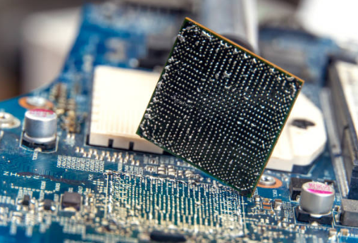
Mixed Technology Assembly combines Through-Hole Assembly (THA) and Surface Mount Technology (SMT) assembly onto the same printed circuit board (PCB), resulting from the increasing number of electronic devices that incorporate both types of assembly. The advantage of this technique is that it can use either surface mount or through-hole components in a single printed circuit board assembly so that the strengths of the two types of technologies are combined. The most apparent advantage of through-hole components across the board is their solderable leads, which provide a robust mechanical connection liable to meet the needs of components with higher power handling or mechanical strength. Meanwhile, the surface mount components offer advantages in size, weight, and cost-effectiveness, among other measurable aspects. The mixed assembly technique is often applied in situations where a number of different components are used to cause a specific type of behavior or function or to achieve a given performance level, giving an option for different design and manufacturing.
Single-Sided Assembly
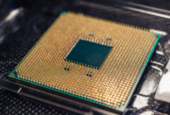
The single-sided assembly, however, is an instance of a circuit board manufacturing process in which only one side of PCB is being populated with electronic components. The construction, which incorporates components either through hole components or SMT assembly approaches that are innovative, is mainly dependent on the state of the art and specific project requirements. The single-sided board assembly technique is often employed in those uses where the size of the printed circuit boards is not an issue and the application space is not a major concern. It enables economies in production through single-side PCB manufacturing without the complexity of a double-sided or multiple copper layers. Meanwhile, though, it will take lead time, reduce the packed density of part elements on the panel and not be an ideal choice for more fixated electronic layouts.
Double-Sided Assembly
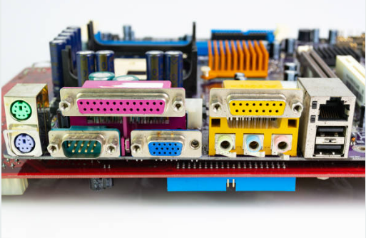
Double-Sided Mounting, on the other hand, is a way of constructing electronic devices in which components are assembled on both the front and reverse sides of the printed circuit bare board (PCB). Using this method, a more component-dense assembly and a greater fidelity of circuit designs can be achieved as compared to single-sided printed passive bare board assembly. In double-sided construction, parts could be mounted using both the through-hole assembly technique and the surface mount technique. The parts could then be placed according to preference and availability. This strategy is most commonly employed when place efficiency is important or if highly complex circuits are required where components are placed on both sides of the PCB. Double-sided assembly requires a lot more care and can also be challenging and time-consuming as compared to single-sided assembly due to the need for accurate and in-time component placement for soldering on both sides of the board. On the flip side, it opens new design possibilities and provides the platform to manufacture all the necessary electronic devices and applications as well.
Multi-Layer Assembly
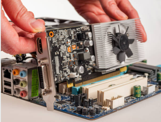
The advanced Multi-Layer Assembly (MLA) method is a modern production technique that enables the creation of PCBs with more than two conduction layers separated by the insulating material. Through the extensions of linings, these layers can make contact through vias that will be useful for circuit designs with high component density and good signal quality. Multi-layer PCBs are a primary component in electronic devices that have little space for expansion and require high processing power, e.g., computers and smartphones. The completion of this assembly process is done using this method. It involves the placement and precision alignment of layers, the drilling of vias, plating with non-conductive substrate material, and lamination. The mounting of elements using these options, including whole assembly (THA) and mounting on the surface (SMT) technologies, offers a range of choices in design and functionalities. Despite seeming to be more complicated, the multi-layer process is basically an inherent property of modern electronic circuitry since it endows improved design flexibility, electrical performance, and reliability.
PCB ASSEMBLY PROCESS
The PCB (Printed Circuit Board) assembling activities consist of several stages, during which the functioning of an electronic circuit is ensured.
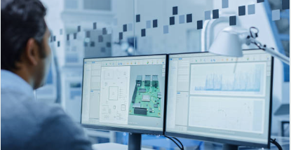
Design: Most commonly, the process begins with designing the PCB layout by using computer-aided design software (CAD software). It entails deciding on the layout of components and figuring out the trace routes. and making sure that the electrical connections are correct.
Component Procurement: The next step is to complete the design and this includes sourcing parts from suppliers. The above components are resistors, capacitors, integrated circuits (ICs), connectors, and many others.
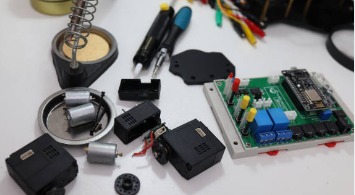
Stencil Creation: For SMT-type of assembly, stencil is being produced which is based on design of the PCB. This is a stencil to be used for solder paste application on the PCB.
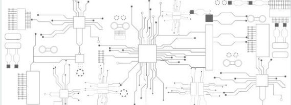
Solder Paste Application: Solder paste, which is an admixture of tiny solder balls and flux, is transferred to the suitable areas of the PCB by means of a stencil. The grass print is made by a stencil printer.
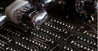
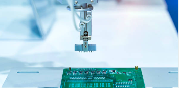
Component Placement: Autonomous pick-and-place machines with the aim of precisely placing the surface-mount components on their proper location on the PCB will be used. The work involves the insertion of SMT components, which usually happens manually.
Reflow Soldering: The reflow oven is used to heat the PCB with the components and the solder on its surface. In the oven, the solder paste melts, following which the joint of solder and bare boards is created, supporting the components to the board.
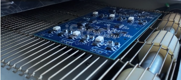
Inspection: Inspecting the soldered PCB after soldering operation is done to determine the manifestation of different kinds of defects, e.g. solder bridges, missing components or components misaligned. Automatic optical inspection (AOI) and X-ray inspections are, respectively, quite frequent methods.
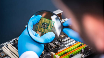
Testing: The functional testing procedure demonstrates whether the PCB with all components in place operates as designed. Such steps may include electrical tests, programming (when applicable), atmosphere tests, and so on.
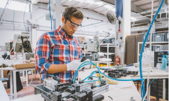
Cleaning: The soldering procedure generated some flux residues, which were removed by cleaning the previous PCB. Such reliability requires not only strong materials but also prevention of corrosion and a lower risk of other problems.
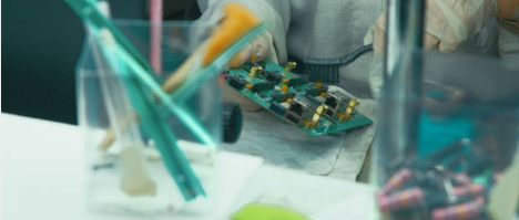
Quality Control: Throughout the assembly process, a number of quality control measures are put in place to test the reliability and functionality of the PCB. This encompasses such parameters as care for the accuracy of placing the components, the quality of the solder screen, and electrical features. Any discrepancies arising in specifications are pointed out and sorted out with immediate effect, as quality is our paramount concern.
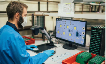
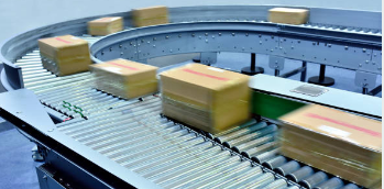
Packaging and Shipping: After final shipment of the PCB assembly clears quality control, it will be packed based on customer demands and wherever necessary, it will be packaged properly for shipping.
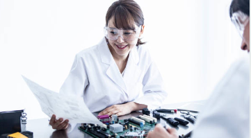
Documentation: Detailed documents, including component assembly instructions, bills of materials (BOM), and test reports, are enclosed with the PCB board assembly. This simply meant that any issues that emerged in production or the product lifecycle at a later stage could be followed up and fixes given thereto.
Common Electronic Components Used in PCB Assembly
In the assembly process of the printed circuit boards, a range of electronic components are used which render particular features of the circuit design.
Resistors
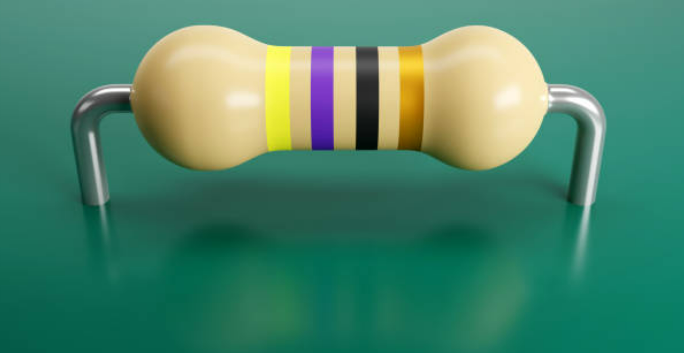
Resistors are installed in circuits to regulate the flow of electricity, reducing currents and their levels.
Capacitors
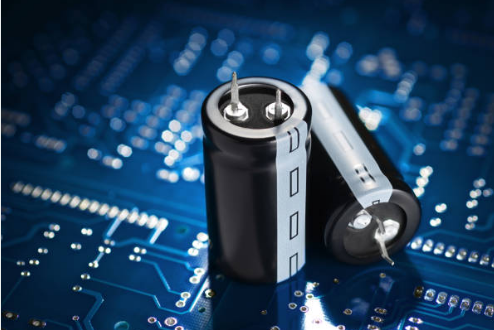
Capacitors act like reserves of energy, which are either stored or released into the circuit and are fundamental for filtering, smoothing voltage waves or coupling signals.
Diodes
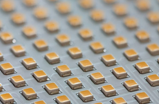
Diodes are unidirectional current element that mainly used in rectification, demodulation of signals, etc. In addition, it also acts as a voltage regulator.
Transistors
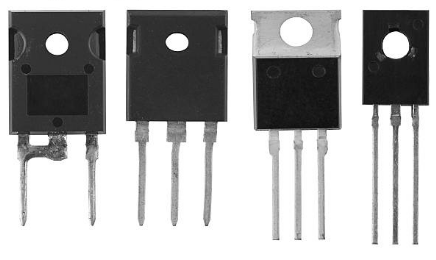
Transistors are semiconductor amplification, switching and signal modulation devices used for in electronics circuitry.
Integrated Circuits (ICs)
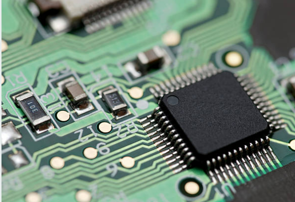
ICs are composed of several discrete electronic elements (including transistors, resistors, and capacitors) that are nested and connected onto a single package. They are utilized for a quite vast range of purposes, which comprise micro processors, memory, amplifiers, and digital signal processors.
Inductors
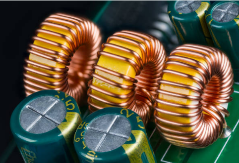
Inductors maintain energy within magnetic fields and are applied to circuits as filters, energy storages, and signal processors.
Connectors
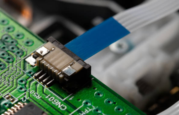
Connectors have a physical and electrical role in providing connections between interconnecting PCBs and other electronic components, which in turn allows the transfer of signals, power, and data.
Switches
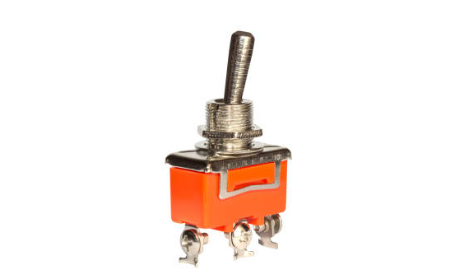
Switches can control the direction of the current in the circuit and by simply turning them on or off, they can be used for turning devices on or off, selecting between different circuits and even controlling functions.
LEDs (Light-Emitting Diodes)
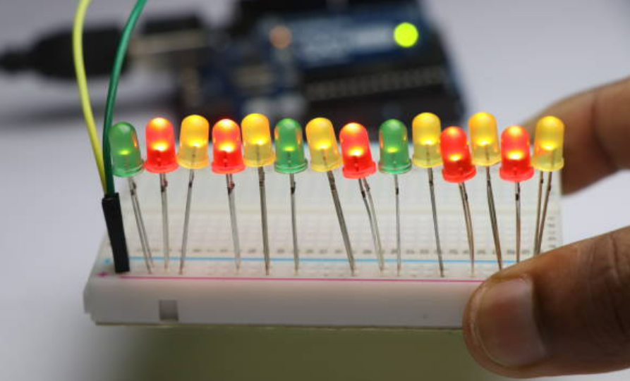
LEDs generate light when it carry out a current through their small diodes. LEDs are used for indication, display and lighting purposes.
Crystal Oscillators
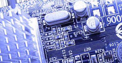
Crystal oscillators provide high-precision frequencies utilized in timing and synchronization functions of digital circuits, usually microcontrollers and communication systems.
Voltage Regulators
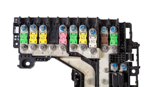
Voltage regulators will keep the output voltage steady irrespective of the input voltage fluctuations or the load current fluctuations, and this allows constant bellow appliance operation.
Transformers
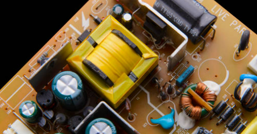
Transformers transform voltage levels up or down in AC networks and communicate them through converting voltage and isolating.
What Equipments is being used during the PCB Assembly Process?
The manufacturing process of PCBs (Printed Circuit Boards) utilizes machineries and mixed assembly, each of which carries the respective responsibility.
PCB Fabrication Equipment
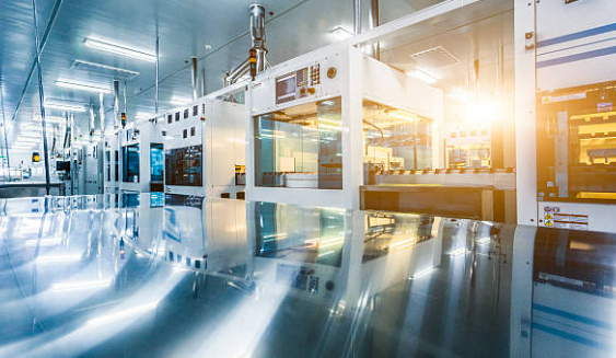
CNC Machines: Application of Computer Numerical Control (CNC) means using it for the creation of accurately drilled holes that are usually into a fiber-glass-reinforced epoxy-laminated substrate.
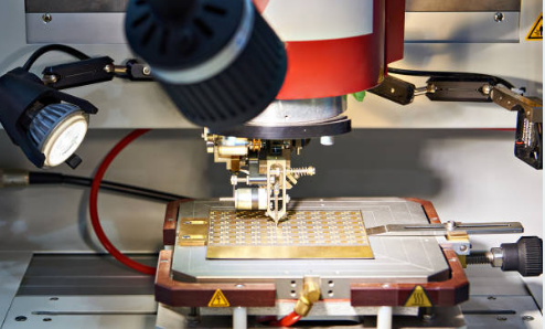
Etching Machines: Etching machines separate the copper underneath the surface to leave a structure in the form of suggested design. By means of acid etching or plasma etching, a more accurate characteristic lines resolution can be obtained.
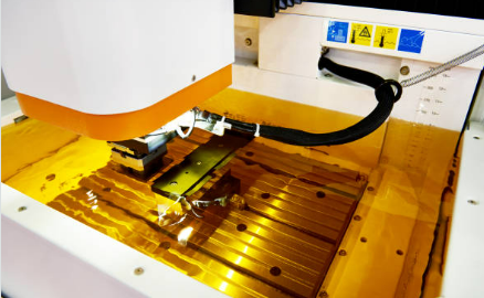
Laminators: Modern laminators are used to combine different layers of substrate PCBs and laminates to enable manufacture of multilayer PCBs.
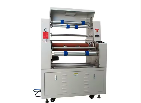
Plating Equipment: Plating equipment serves to deposit metal film (mostly over copper) into the drilled positions and onto the printed circuit board surface to create conducting pathways and pads.
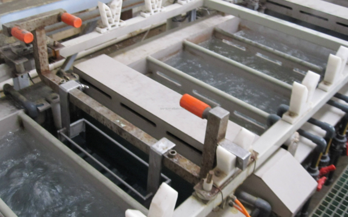
Solder Mask Application Equipment: Solder mask application equipment is employed to cover a thin film of solder mask material over the surface of the PCB, thereby shielding the copper tracks from oxidation and likewise allowing the soldering process of association to proceed smoothly.
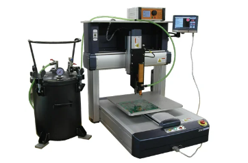
Surface Finish Equipment: The surface finishing machine, at the end of the through-hole process, covers or coats the copper surface of the PCB on both sides to enhance its solderability and safeguard it against oxidation. Surface finish techniques such as HASL (Hot Air Solder Leveling), ENIG (Electroless Nickel Immersion Gold) and OSP (Organic Solderability Preservatives) are widely applied in the process.
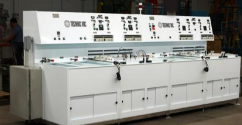
PCB Assembly Equipment
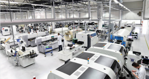
Stencil Printers: Solder stencil printers are used for pasting solder over the surface of the printed circuit board, defining the respective contact locations of the components that will be mounted on it.
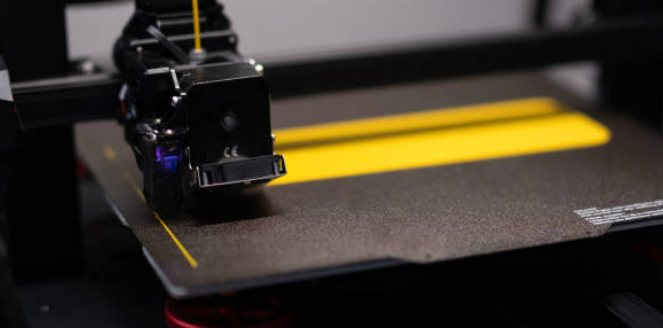
Pick-and-Place Machines: Pick-and-place robots, or pick-and-place machines, are a type of robotic system which accomplishes the mechanical placement of surface-mount components onto the PCB with the help of vacuum nozzles. These machines reduce the complexity of the assembly process by taking care of many variables, such as the size, shapes, and speeds of the PCB components. They make the assembly faster.
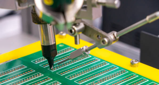
Reflow Ovens: In reflow ovens, the solder paste on the surface-mount components melts above its melting points when temperature of the assembly is higher than the melting point of the solder paste. These steps of selective soldering ensure excellent joints between the part of the circuit and the PCB.
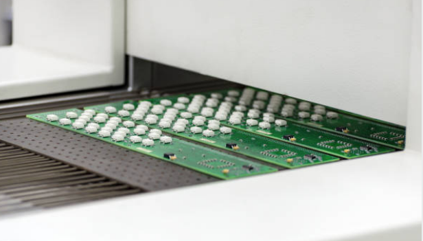
Wave Soldering Machines: Wave soldering may be referred to as the traditional soldering technology which is used for soldering through-hole components. Eventually, the PCB will be laid in the influx of molten solder, which will create solder joints betweenthe through-hole components and the PCB.
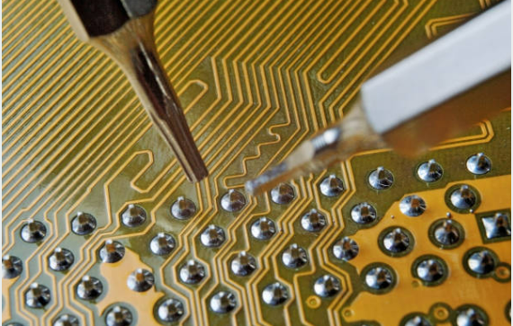
Inspection Equipment: Inspection equipment, including Automatic Optical Inspection (AOI) machine as well as x-ray inspection systems, can be used to find defects like solder joint failures, component misalignments, and shorts or open circuits.

Testing Equipment: Inspection tools are used, whereupon you can track the level of a setup’s function and electrical performance of the finished PCBs. It may involve functional testing, in-circuit testing, boundary scan testing, and other tests, depending on requirements of the system.
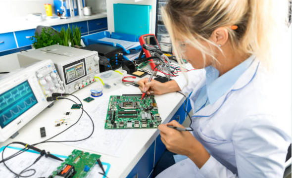
Tips for Choosing Components in your Printed Circuit Board Assembly
Component selection for the PCBA (Printed Circuit Board Assembly) is a vital stage which can make a difference in the degree of product performance, cost and reliability.
- Functionality Requirements: It is essential to define how your product should perform as well as its functionality requirements. Since then, you will be able to figure out the types of components required and all the various kinds of specifications that accompany them.
- Component Specifications: Carefully watch out for the particular characteristics of each component, like the voltage ratings, current ratings, tolerances, operating temperature ranges, and package sizes. Make sure that chosen component standards are at the level of your design and not even below it.
- Quality and Reliability: Pick parts from those manufacturers that are well-known, particularly for their hard quality and reliability. Take precautions to ensure that you don’t invest in fake parts or inferior-quality ones because they can cause premature breakdowns and costly recalls.
- Availability and Lead Times: Take into account the instances in which components are available as well as the time needed for production delivery if your production deadline is particularly tight. Pick parts from distributors who offer them from multiple providers to keep the supply chain intact.
- Cost Optimization: Strike the balance between component cost and other budgetary sources of your project. Establish the possibility of determining cost savings through an evaluation of prices of the same items from various suppliers and replacement of components with similar performance.
- Lifecycle Considerations: Think over the whole lifecycle of the parts, particularly for large projects or items with long service life. You may also find the following instructions useful: Humanize the given sentence. Select components that will be available whenever needed and are expected to have long-term production, as they may help you avoid obsolescence.
- Compatibility and Interoperability: Make sure that the undertaken components are part of a scheme that is suitable to work with other design components and industry-standard interfaces and protocols. This type of immediate testing is critical to making sure essential parts like micro controllers, sensors and communication devices work.
- Environmental Considerations: Consider environmental factors like temperature, humidity, impaction, vibration, and environmental factors to a large extent when choosing components, mostly for extreme applications. Find qualifying components with acceptable environmental ratings and certifications.
- Documentation and Support: Choose items that accompany good support materials, such as a datasheet, application notes, and technical support documentation. The device should be used for rectification, inter-connection, and problem solving of your project.
- Future Scalability and Upgradability: While selecting components, remember to keep the scalability and upgradability requirements in mind that will signify the future. Choose details that make it easier to combine a variety of new features, create extra functions, or update to more efficient versions.
Implementing all of the tips mentioned here, which also include extensive component analysis coupled with evaluation, ensures that you get an acceptable, cost-effective, and high-performing PCBA for your electronics device.
CONCLUSION
In conclusion, a PCB assembly is a crucially significant step in PhEOS circuitry making process that consists of smearing the bare printed board with electronic components to produce operating electronic circuits. The assembly is a multistage process which consists of solder paste application, placement of the components, soldering phase, inspection, testing and tape and reel packaging in most of the cases to lead free rohs. The virtue of the prototyping of the printed circuit boards is to ensure the product’s reliability and customer satisfaction, minimize the manufacturing costs, meet standards and rules, improve the production process, prevent risks, and maintain a reputation and consigned assembly.
Manufacturers may carry out quality control measures effectively and enable the use of latest manufacturing technologies to deliver outstanding PCB assemblies which satisfy the needs of customers better and exceed industry standard also in plated through hole. Finally, PCB assembly is one stop solution what makes the whole electronic device production a greater reality for operation, including the innovative consumer electronics and the advanced equipment used in the industrial sector, which is one of the crucial elements of the electronics technology development.

