Printed Circuit Boards (PCBs) are the heart of all modern electronics that built the network of wires which carries electricity through everything from the smartphone to the space satellites. Notwithstanding the same, the product of design which is PCB is likely to be subject to some issues one of the main ones being delamination. Hereby, a blog post is presented on what is the main cause for PCB delamination, what causes it, and how the situation can be avoided to preserve the functionality and reliability of electronics.
What is PCB Delamination?
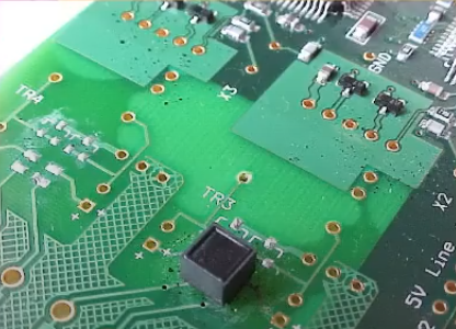
The phenomenon called delamination in the PCB occurs when an aged or poorly processed circuit board starts to separate into layers. But in the latter case the material may be placed between the copper foil and base material or even within the base material itself. Flashbacks are usually in the form of bubbles or blisters that are seen on the substrate surface of the PCB and can be very vital to the proper workings of an electronic device and this in turn causes failures in function.
Causes of Printed circuit board Delamination
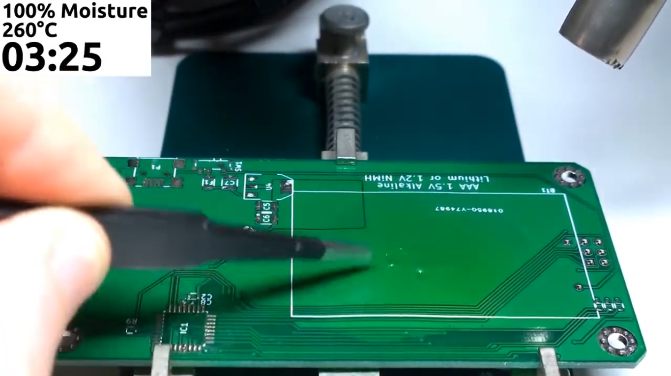
Several factors contribute to the delamination of PCBs:
1. Excessive Heat During Manufacturing
Delamination is often the result of the most prevalent factor in the etching and soldering process overheating. In case of subjecting the inner layers of the PCB to higher temperatures that are difficult to bear for materials, the layers expand at different rates and separate in order to survive.
2. Moisture Entrapment
A moisture-filled environment can be encountered in the course of production process of fabrication as well as when the PCBs are being stored. When heated, this moisture transforms to steam which can drive the layers separate where they were bunched together.
3. Mechanical Stresses
These processes can put physical stresses on the composite parts too. The stresses come as a result of bending or twisting which may occur inorganic materials during the manufacturing, installation, or even use.
4. Chemical Contamination
The effects of contact with harsh base materials such as chemicals degrade the bonding agents used in PCB layers, thus, the layers are bound to start separating.
Preventing PCB Delamination
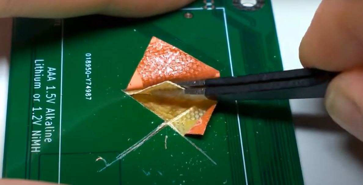
To minimize the risk of delamination, PCB manufacturers and designers can adopt several practices:
1. Controlled Lamination Process
Considering the lamination in a controlled environment and maintaining the lamination with the temperature, pressure and the time period are an utmost necessity in obtaining a strong bond of the layers.
2. Proper Material Handling and Storage
Storing materials in air-dry condition and ensuring proper temperature and preventing moisture by pre-baking materials can be the main preventative measures to take.
3. Design Considerations
The careful positioning of pads on the PCB weave interior with a wide terminal space with not narrow slots and velocity and constant copper balance is the possible way of the prevention of delamination.
4. Quality Control Testing
Introducing scrupulous testing protocols, particularly thermal stress testing that can spot delamination problems the PCBs has, could be done before other elements are put together to create the LCD device.
5. Using High-Quality Materials:
High-quality substrate and adhesive specification that can withstand thermal excursions, dimensional changes, mechanical stresses, and the operating environment must be considered.
At What Temperature Does PCB Delamination Occur?
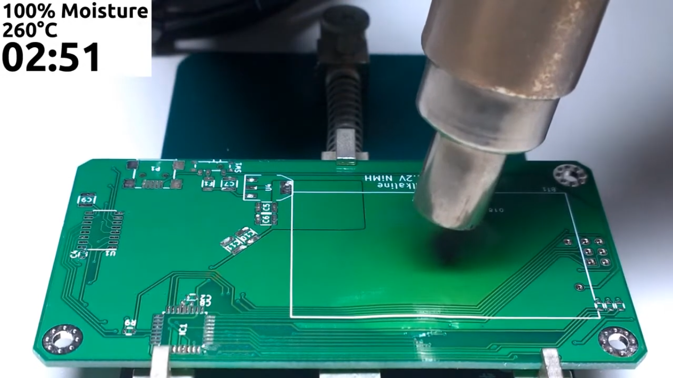
Now, PCB delamination mainly appears when the board is exposed to temperature well above 250 degree Celsius (482 degree Fahrenheit) excessively during thermal processing. Such high temperatures affect the employed materials to swell at different rates, leading to the layers separated. Prevent overheating and potential deformity of the product is mainly promoted through effective temperature control during this stage.
Why Does the PCB Delaminate When Being Reflow Soldered?
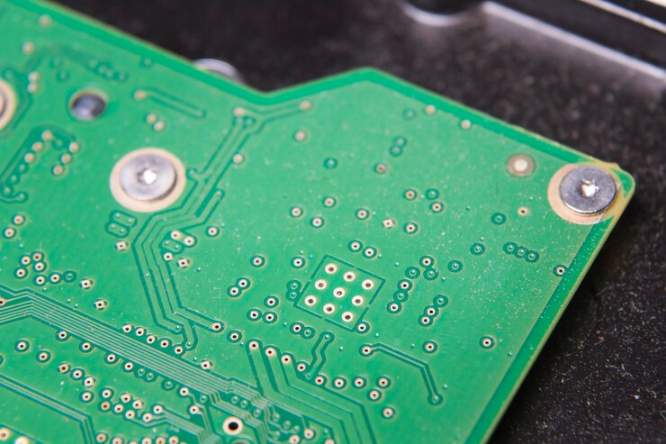
PCB delamination during the reflow soldering is one of the major problems that happen as a result of exposure to high temperature as well as entrapment of moisture within the plate. The water thus transformed at high temperature into a gas of particular kind called steam gives the layered molecules a mechanical pressure that allows them to move apart. The PCB board should be dried at the required temperatures to remove moisture. Moreover, the temperature used during reflowing should be carefully controlled to hinder delamination.
How Can You Tell Whether the PCB Is Harmed or PCB Delamination Has Occurred?
If PCB is damaged or delamination has taken place, these can be easily found out just by looking for the visible signs like bubbling, blistering or layers separation on the surface of the board. Any other sign can be applied by looking at the skim surface of the board or its texture is changed. The functional aspect of this also requires some consideration as you could be dealing with circuit behavior that is unexpected, loss of connectivity, or change of impedance, which all points to the presence of delamination or damage.
Effects and Consequences of PCB Delamination
PCB delamination can lead to several adverse effects and consequences, including:
- Reduced Mechanical Integrity: The PBC’s ability to sustain physical strength is jeopardized, which may invalidate the design’s primary function.
- Electrical Failures: Elevation of blisters that will brake chip paths can lead to open what is referred to as short circuits and overall unreliable electrical performance.
- Thermal Management Issues: An interruption of the heat layer can cause any kind of overheating that may be extra terrific even evolving to damage of the PCB base materials and its very components.
- Increased Repair and Replacement Costs: Such potting compound PCBs may go through a rework process leading to a higher production and maintenance costs.
- Product Failures: In particular, in the critical uses such as the medical or aerospace devices, the delamination can he dangerous and in the worse case, it can cause catastrophic failures of the product, posing safety risks.
Delamination Measurement Tests
PCB Delamination Tests Reliable are what usually involve the deployment of different techniques to find out the state of the overall board and also the retention and fixation with the PCB layers. Common tests include:
- Micro sectioning (Cross-section Analysis): After sample of PCB is cut and polished, it is put under the microscope to observe contact between different layers. We look for delamination appear.
- Thermal Shock Testing: The delamination in the PCB is detected by cycling the PCB into temperatures of extreme humidity since materials expand and contract.
- Acoustic Microscopy (Scanning Acoustic Tomography): This non-destructive examination relies on the use of echoes to detect delamination and other imperfections that fall within the PCB layers.
- Peel Strength Testing: The debonding force required to peel the copper substrate fabric gives the clue to the strength of the adhesive materials.
- Time Domain Reflectometry (TDR): An electric test which is a change in the impedance values resulting from the delamination.
Blistering vs. Pcb Measling
Blistering and Measling are two different types of defects that can occur in PCBs:
Blistering
This is an issue that shows as raised bumps or blisters that appear on the oxide layer of the surface of the PCB, often due to the pocket expansion of the excessive moisture or the gases getting trapped during the process of lamination. It acts on the top layer of board and may be unfavourable to both its mechanical and electric behavior.
Measling
Measling is known to be the presence of some small signs or uncoloured in the resin substrate of the PCB which is observable through the glass cloth layer or glass transition temperature. Most commonly this type of failure occurs either due to microfractures within the resin or breakages between the resin and reinforcements. Measling normally has no functional but only cosmetic effects on the PCB unless it is severe enough resin.
Delamination Repair Steps
Repairing delamination in PCBs can be challenging, but here are basic steps that can sometimes help mitigate the issue, depending on the severity:
- Identify the Delaminated Area: Use visual inspection or non-destructive acoustic microscopy to determine the specific location of delamination.
- Clean the Area: Clean-up the debris and the filth from the torn areas of the laminate.
- Apply Heat and Pressure: Use a selective heating and pressurization coupled to the affect areas. The process involves the use of equipment that is usually designed for this specific purpose.
- Curing: Letting the fix adhere after curing in a controlled environment, achieving uniformity of the layers and plentiful bonding.
- Testing: Electric and mechanical test of the repair are required to ensure the PCB is still logical and functionally abides by the technical specifications.
Conclusion
Delaminations are a kind of problems very dangerous, which able to decrease the overall performance and value of these boards. Through identifying its root causes and applying robust prevention techniques against poor manufacturing processes, manufacturers are able to in fact, dramatically mitigate the chances of delamination and thus commercialize their lasting products to the ultimate users. With the technology becoming more advanced everyday, robust PCB design and manufacturing processes will carry significant importance, so these preventive measures will move to more of essence than ever.

