In the modern arena of electronic product quality making, precision has become an essential part. With technology expanding and modern printed circuits becoming more complex, it is imperative to assure that each part is properly assembled and soldered. This is where automated optics inspection (AOI) takes its place—a tool that is the blazon of standard quality. Here, you will find an exploration of the AOI technique, the way it works, and the significance of its use in modern manufacturing.
What is Automated Optical Inspection (AOI)?
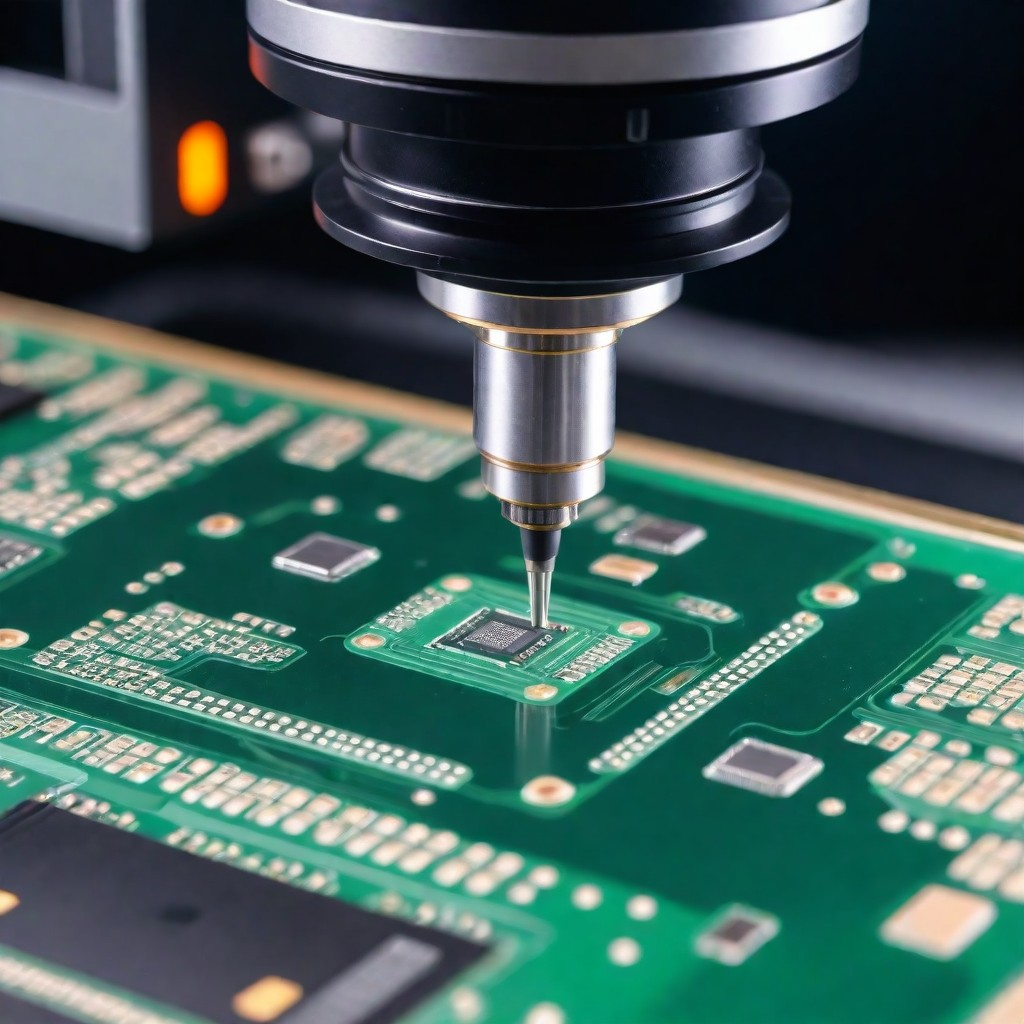
The use of Automatic Optical Inspection (AOI) technologies as an approach to visual inspection printed circuit boards (PCBs) at their assembly phase has dramatically simplified the procedure in the manufacturing system. It makes use of a mix of cameras and light control systems that take snapshots of a chessboard, while its advanced software carries out the mathematical analysis of these images. AOI is aimed at presenting the smallest errors or area defects possible as early in the production line as possible, to stop the issue from even reaching the final assembly or the consumer`s hands.
Here are Some of the Key Points about Automated Optical Inspection
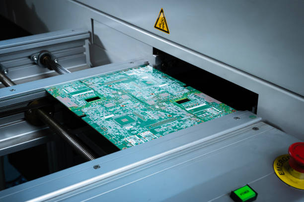
Automated optical inspection (AOI) is a crucial tool in PCB manufacturing, offering several key benefits:
- Accuracy: AOI systems enable very good sensitivity in detecting defects like soldering errors, incomplete components, or misalignment.
- Speed: These devices can examine printed circuit boards (PCBs) with the Swift system, which will considerably reduce the production process time because manual inspection is very slow.
- Consistency: AOI provides a consistent quality level as errors and fluctuating outcomes are replaced by a machine.
- Documentation: It automatically does the note-taking for test data, which really helps to control the quality in case of any issues.
- Cost-effective: Even if the first investment is quite high, the evaluation of AOI enables a decrease in production costs as far fewer defects are created and also less rework.
- Scalability: AOI systems are scalable and, thus, can easily integrate into different PCB processes and complexity levels; hence, they can be used for production line volumes of different amounts.
Importance of Automated Optical Inspection in Modern Manufacturing
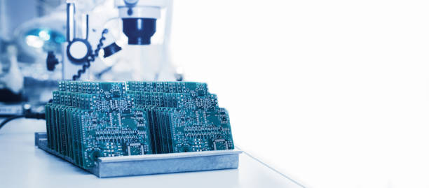
Automated optical inspection (AOI) is vital in modern manufacturing for several reasons:
- Quality Assurance: The AOI provides better quality control and defends unmanufactured products by detecting defects early in the manufacturing process.
- Efficiency: With ongoing item inspection at high speeds, it allows to minimize equipment downtime and throughput lags remarkably.
- Cost Reduction: This process in monetary terms translates into the reduced cost of reworks and waste, with the former being further down the line and the latter being entirely avoidable, directly leading to cost savings in the medium and long term.
- Scalability: AOI systems can process large order quantities, meaning they are fit for scaling production without performance affects.
- Consistency: It guarantees high-quality consistency using processes that are repeatable and accurate, hence making products with standardization as a result.
- Integration: The human-machine interface is one of the features of AOI capable of being efficiently integrated with automatic systems, greatly contributing to the progress of automation and smart factory movements.
This is why its use is an integral part of modern production in the challenging environment of global competition.
How does AOI work?
Automated Optical Inspection (AOI) employs cameras to inspect PCBs visually for defects. Therefore, it is possible to identify defects on printed circuit boards through automated optical inspection. It contrasts the printed images with a sophisticated schematic to locate possible discrepancies like missing components representation of components, misalignments, and soldering faults. This approach is aimed at validating the PCB assembly so that final products can be assembled correctly.
Optical Systems in AOI
The optical systems of AOI machines provide highly detailed photographic images, which are used to locate and report defects in this process. Here are some key components and advancements in the optical systems used in AOI:
High-Resolution Cameras
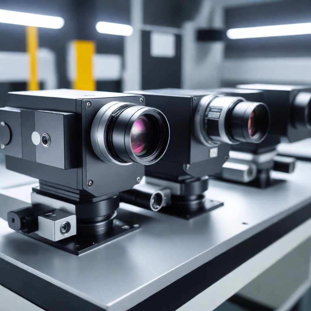
Advanced AOI machines include high-quality camera systems that capture not only the detailed images of the PCB’s but also provide a wide range of field of view. These cameras effectively confirm small defects like soldering errors, component drift, and replacing missing parts. Hence, we cannot live without these cameras for any production line monitoring. The resolution of such cameras is constantly improving, making it possible to use the cameras to find finer details and perform analysis of these details.
Multiple Camera Systems
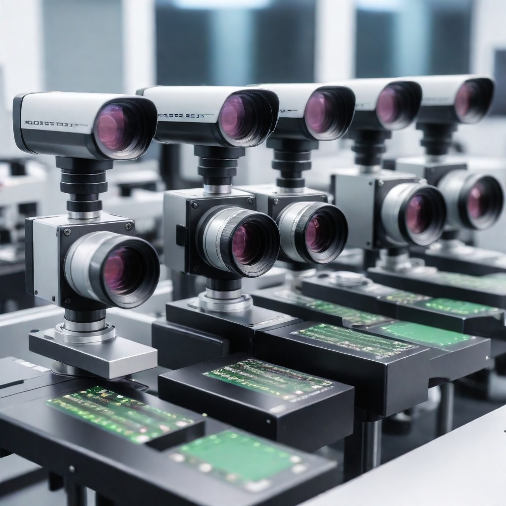
Different AOI machines are now making use of many cameras or combination cameras at different angles to track the entire PCB view. Tempering is characterized by defects, namely those that are hidden from only one camera. This arrangement is efficient for poring over a complicated printed circuit board that covers multiple layers and other boards.
Advanced Lighting Systems
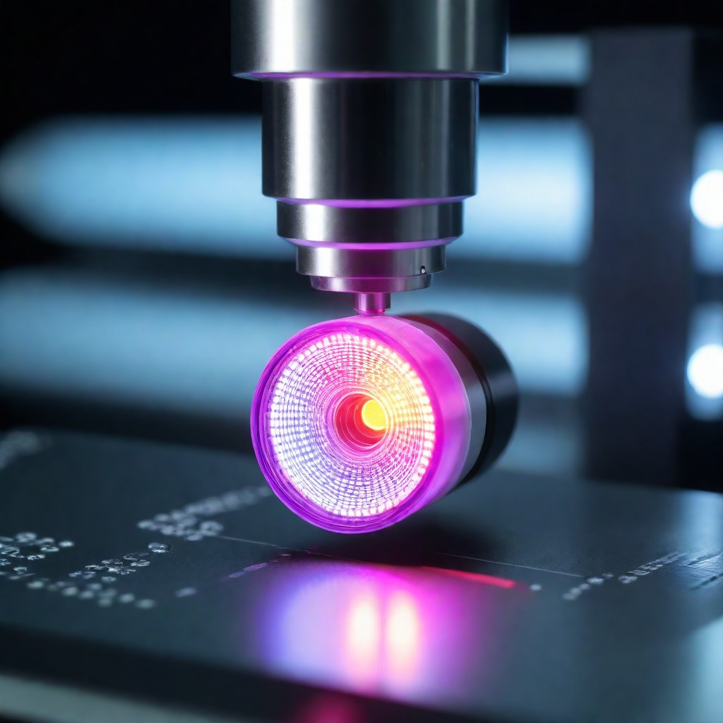
Lighting that is suitable for optical sensing is necessary and imperative for inspection. AOI systems apply lights that range within different kinds of light source—LED, fluorescent, and sometimes specialized lighting—in order for different kinds of defects to show up. The lighting setup is able to be adjusted to match the needs of the inspection and emphasize the inspection faults or surface features.
Image Processing Software
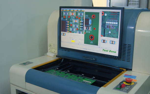
The images are captured, and the smart software analyses them by comparing them with templates or downlines. Story: This intelligence software can recognize any tiny deviation from normal and flag potential problems. Among the most exciting developments is the making use of machine learning applications that help augment the precision and speed of fault detection.
3D Inspection Capabilities
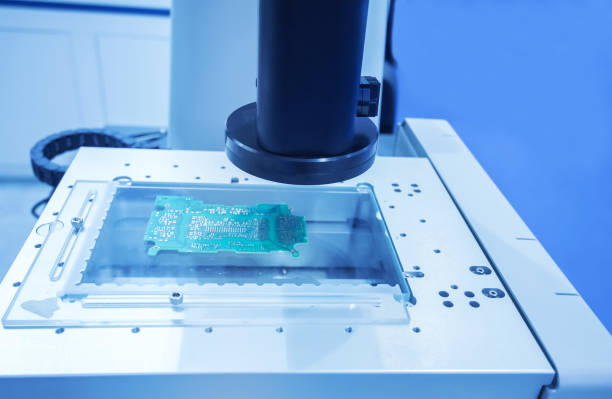
Strong limits of 2D imaging are now removed by the implemented 3D inspection facilities in many modern AOI systems. Such systems involve the use of technologies like laser profilometry or the stereoscopic imaging method to measure the height of components and solder joints, detecting parameters that indicate problems such as irregular or insufficient solder joints or insufficient paste solder volume.
Several types of software algorithms commonly used in AOI systems
These algorithms thus increase the capacity of the AOI systems, which allows them to deftly identify defects with high accuracy, minimize the chances of false positives, and improve the reliability of the inspection process.
Modern Automated Optical Inspection (AOI) systems employ various sophisticated software algorithms to enhance inspection accuracy and efficiency.
- Deep Learning Algorithms: These are the ones which are employed for the purposes of identifying intricate defects in electronic devices Convolutional Neural Networks (CNN) are one example of deep learning models that are used in computer vision systems. The deep learning models are trained with large data sets to understand an extended range of defect types in them.
- Template Matching: The conventional approach is based on the side-by-side comparison of the acquired images to a previously stored image of an assembly with no mismatches or defectant parts.
- Statistical Pattern Recognition: A statistical approach measures the patterns and creates suitable adjustments against the variations in images. This helps to maintain high quality and avoid being flagged for every minute deviation.
Implementation of AOI in Manufacturing process
The Automated Optical Inspection technology is a vital tool, which is used widely in the production process, mainly in the electronics manufacturers, to facilitate the quality control process. Here’s a concise overview of how AOI is implemented in manufacturing:
- Integration into Production Line: AOI systems are usually placed at some strategic points on the production line and those key points are often after soldering of a solder paste, pre-reflow, and post-reflow phases in circuit schematic of a printed circuit board assembly circuit.
- Visual Inspection: The device employs high-pitch cameras to make all-round images with finely of the product. Such pictures are analysed by using highly efficient software systems so as to facilitate the identification of the defects.
- Software Analysis: The software reviews the taken images against a highly sophisticated image reference, the golden board (a board with no anomaly), to point out imperfections like misalignments, component missing and bad soldering.
- Immediate Feedback: The defects are detected a once AOI system and then started working either for the imperfections from the operator`s side or from in the production machinery. By means of this, quick responses are obtained to be guiding and correcting, leaving no room for the evil of fragmentation and reworking.
- Data Collection: AOI systems (Alternative of actual observations systems) collect manufacturing data, which can be used for a number of purposes like improving process control, predicting possible failures, and enhancing overall product quality.
Different Types of AOI Systems and their Pros and Cons
AOI (Automated Optical Inspection) systems are key tools in manufacturing especially electronics, to find out problems such as a faulty printed circuit board (PCB board), components or assembled parts. There are different types of AOI systems, each with specific advantages and disadvantages, suitable for varying manufacturing requirements:
1. 2D AOI Systems
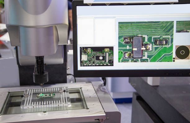
Automated Optical Inspection (AOI) machine comprised of 2D in the electronics manufacturing facility.
Pros:
- Cost-effective: Typically cost is less than other assembly stations.
- High Speed: Which opens up or open circuits possibilities for applying advanced technologies such as 3D scanners, enabling high-volume production lines.
- Simple to Integrate: Simplified manner of assembly for the post production that may be eased but due to lower complexity of the technology required.
Cons:
- Limited Detection: May fall short to catch problems that are not apparent through top view, for example, to find lifting pins or underlying problems.
- Flat Images: A relationship between the 3D and 2D images is not perfect, displayed in some cases of defects in terms of accuracy.
2. 3D AOI Systems
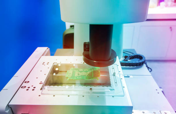
Creation of 3D automated optical inspection automation to be used on the electronics factory line as an example.
Pros:
- Comprehensive Inspection: Employs a laser scanner or other technologies to measure the package height and solder joints and verify the filled package or find subtler flaws like lifted leads or insufficient soldering.
- Higher Accuracy: Has the ability to deliver secondary defect detection by generating an ultra-high detailed 3d image of the PCB.
- Better for Complex PCBs: Suitable for inspecting through-hole or multi-layer PCBs, it is gifted with such resolution as to reveal tiniest defects.
Cons:
- Higher Cost: Cost more than 2D systems, owing to the advanced technology required.
- Slower Inspection Speed: The 3D printing tech, typically takes longer to fulfill than 2D systems might cause a drop in the output in high-volume intentions.
3. Inline AOI Systems
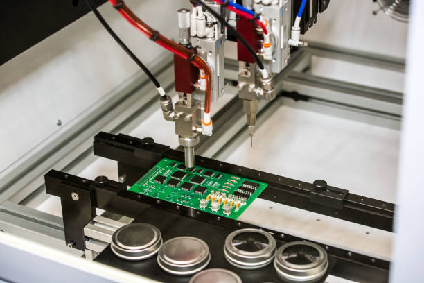
Pros:
- Integrated into Production Lines: Provides opportunity for in-time monitoring. Which improves quality control during the manufacturing line width violations
- Immediate Feedback: The platform provides direct input to development, allowing for acknowledgment and fixing of process errors when the latter still can be affected.
Cons:
- High Initial Setup Cost: Expensive to establish because of the necessity of producing the special parts.
- Can Disrupt Production: Despite representing good control, best condition of the line depends on its optimum operation.
4. Offline AOI Systems
Election of offline Automated Optical Inspection (AOI) system in electronic manufacturing application.
Pros:
- Flexibility: Compared to traditional conveyor assembly lines, the robots can be placed at any stage seamlessly without changing the production setup.
- Cost-Effective for Small Batches: The flexibility of going beyond the main stream and makes them suitable for prototypes or low-volume production lines where the integration is indispensable.
Cons:
- Manual Intervention Required: Usually manual loading and unloading of boards-this involves labor and time which are input workers.
- Less Immediate Impact: It does not allow you to respond in the same way as a realized system.
Each of these semiconductor devices contributes some specific aspects that it is good at, and yet, it also has its own individual failings. Is it THT or SMT depends on the particular manufacturing requirements, which could include quantity per batch, the complexity of the PCBs and costs. For higher-lager and more-complex productions, the 3D-ie and inline AOIs are more beneficial, because of their wider range of detection, despite commencing their expenses, the systems can be integrated into process lines and can control the quality during real time processing. Instead, 2D and the systems that are offline could be more suitable for simple applications or production process for lower volumes because of their low cost and the short setting up.
Role of AOI in Quality Control
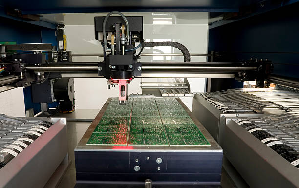
Automated optical inspection (AOI) in quality control can be succinctly described through its key roles:
- Defect Detection: Capable to automatically discovers design faults such as misalignment or imperfect soldering line on printed circuit boards so that products are free of errors when they are assembled or our customers receive them.
- Real-Time Inspection: Performs audits of the facilities during production, which helps to stop flaws with other products on the spot.
- Consistency: Eliminates variance within inspections, and helps reduce mistakes caused by humans, hence improving the quality of products.
- Process Improvement: Data analysis from defects helps to tune manufacturing methods, which results in the production of products with fewer faults and better productivity.
- Cost Reduction: Offers design review at each stage of the production, so that errors are spotted early, which in turn, allows for saving budget on manufacturing.
- Scalability: While it is able to product which is developed to new product lines or changes in product design with minimal alterations it is appropriate for the fast and flexible manufacture.
After all AOI systems plays a significant role in keeping and improving the necessary high production and quality standards and performance in production systems, in manufacturing branches where perfection is the goal.
There are a few common soldering defects that AOI can check
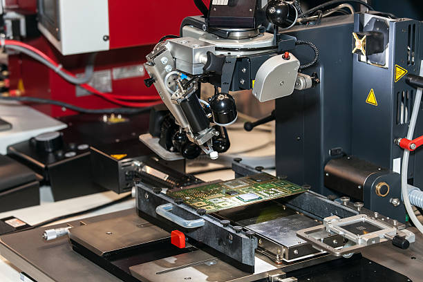
Automated Optical Inspection (AOI) systems are powerful tool to inspect possible soldering defects during the fabrication of printed circuit boards commonly seen and used. These defects include:
- Solder Bridges: An AOI system provides the capability to identify the conductive pads which cause the undesired solder joints, working on the short circuit principal.
- Insufficient Solder: The coplanarity systems are able to identify soldering joints with absent or too low solder volume which may lead to consequently weak mechanical and electrical connections.
- Excessive Solder: The solder running excessively on a joint can create problems like short circuits or generally, it can cause poor performance of nearby components.
- Component Misalignment: AOI is clever enough to detect the component skew that are not planned the right way, that maybe ultimate poor connections or mechanical stress on the joints.
The AOI systems’ capabilities make the whole process of quality control dependable and let operators see if defects are present in a short period of time, therefore, they provide fast, sure, and exact inspections, in addition, they help to avoid more defective products from being further on the production line.
How does AOI compare with other inspection methods?
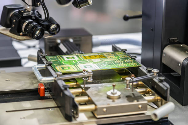
Every inspection scheme has its own benefits that it provides and is chosen based on the operational environment requirements of the particular production area, aspects like, volume defects produced, complexity of the PCBs and the sort of defects that are to be detected some don’t have non contact test method or population tests.
AOI Hardware and Software
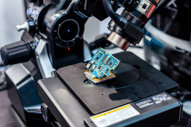
AOI Hardware:
- High-Resolution Cameras: Capture accurate pictures of the cars for the boards detection of errors.
- Lighting Systems: Adjust the position of the headlight to ensure uniform lighting and distinction between images. Use our AI to write for you about any topic!
- Precision Stages: Adjust by PCB board under the camera with the highest accuracy and smooth movement for fine inspection.
- Sensors: Discover several features such as appearance of elements and their positions.
AOI Software:
- Image Processing Algorithms: Perform deviation analysis on patterns by comparing images with the established norm.
- Machine Learning Capabilities: Enhance defects identification even over the time by being able to benefit from previous inspections outcomes.
- Data Management Tools: Organize and store information related to inspections for any need of trend analysis, quality control and so on.
- User Interface: Thus, it gives an opportunity to run the test, to adjust the parameters, and to take measures if any problem occurs.
With more advanced equipment, capture a variety of the visual information. Software on the other hand use this information to achieve smarter defects detection, which is crucial in modern manufacturing.
Benefits of Using AOI
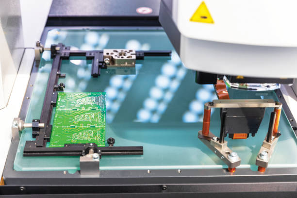
- Enhanced Quality Control: Through AOI stand we offer comprehensive inspection solving PCB’s inspection problems usefully and effectively. Doing so enables early detection of defects which ensures that there is reduction of reworks as well as an increase in the value and integrity of the product.
- Increased Throughput: Automated systems supplant the routine inspection procedures because they work many times faster and uniformly than manual inspection systems. Such high velocity and promptness lead to greater number of garments completed in a shorter timeframe and hence fast/shorter production times without inferiority to quality.
- Reduced Costs: Early defect detection can spills over to the overall reduction of cost implications involved in the return of defective products to market, that is, recall of products and the brand reputation. Furthermore, this will reduce human error and automation of routine activities that can result in cost savings.
- Data Collection and Analysis: AOI systems are the source of large amount of data that can be interpreted to recognize pattern, improve emergence processes, and take decisions to produce manufacturing .
Challenges and Considerations
Along with many advantages, there are bearings to relate to. As for instance, installing an AOI system might be expensive and complicated enough taking into consideration on the initial demand for additional equipment and software. Besides, though AOI is exceedingly precise, no techniques are errorless therefore must be accompanied with other possibilities to ensure the best results.
Evaluation of performance of AOI will greatly depend on the quality of the language processing and precision levels of inspection. Fine-tuning these settings hugely important many times even demanding for having the systems be worked by professionals who will ascertain a system works properly.
Conclusion
Automated Optical Inspection represents a great innovation in the field of electronics manufacturing as it combines the unsurpassed speed, accuracy, and efficiency of manual inspections, which are a white swan on a sea of electronics manufacturing. Alongside PCB`s ongoing growth of complexity, the role of AOI will keep on expanding as a result also some using artificial intelligence. Leveraging this innovation enables manufacturers to emphasize on their quality control processes, cut cost and stay ahead in a dynamic technological environment which is ever changing. While it might seem like that, putting AOI into practice appropriately is the essential part for any electronic firm that wants to be progressive.

