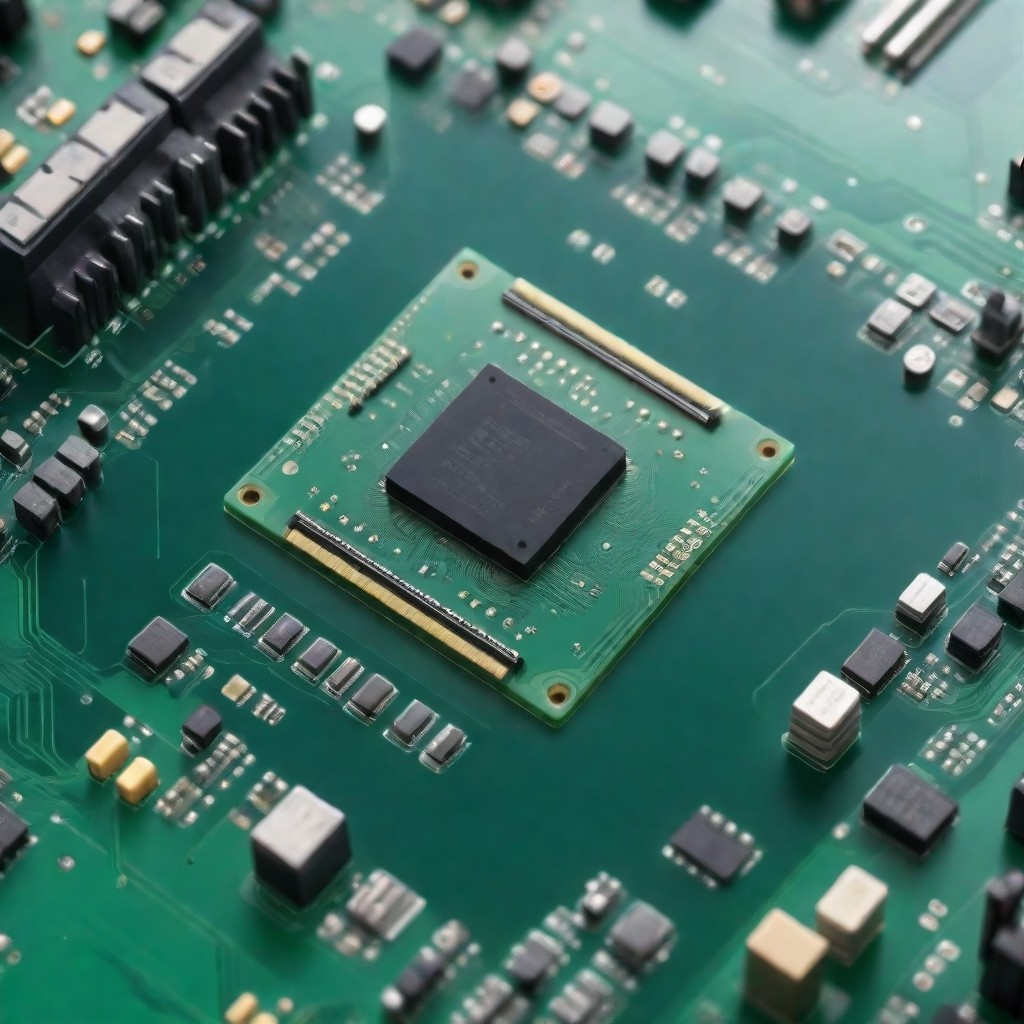
HD (HDI) printing technology is already creating a challenge for designers by reshaping printed circuit board (PCB) designs. The increasing industry needs for very compact, fast, and performing computer and electronics products are likewise totally dependent on the use of HDI PCBs. This particular blog is focused on learning the important techniques as well as taking a look at the most outstanding trends related to HDI PCB design in order to help attain the ultimate goal of elevating engineering and designing projects.
What is HDI PCB Design?
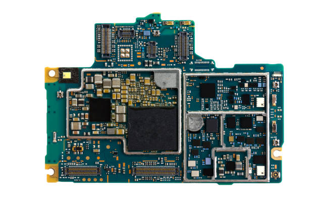
High-density interconnect (HDI) PCB design involves obtaining properties of printed circuit by applying the technology of high-density interconnection. They feature a greater wiring density per unit area in comparison with traditional ones, thereby allowing them to be more multifaceted and compact. HDI PCBs basic functions involve high-density elements such as microvias, extremely thin lines and spaces, and top-performance thin material. With this, the circuit board or printed circuit board is more compact, efficient, and high-speed, which is required for modern electronics like smartphones, tablets, etc.
Techniques for Mastering HDI PCB Design
These are the techniques needed to manage high-density interconnection.
1. Utilizing Advanced Materials
Judging the correct base materials is the key component of municipal structures. These materials also physically demonstrate higher dielectric constants and higher thermal endurance, which ensure their positioning ahead of traditional low-cost resins and glass. The above-mentioned materials will help in getting rid of signal loss and handling heat that exists in dense circuits.
2. Implementing Microvias
Microvias are very small vias that normally have diameters ranging from 0.001 to 0.006 inches. They can be simply a metal sheet or buried, serving the important function of producing multiple-layer printed circuits. Microvia holes reduce board space and thin-out to inner copper layers stacking at the same time, allowing for shorter signal traces and easy current flow throughout.
3. Employing High-Precision Photolithography
Alongside the photolithography of the HDI PCB process, the accuracy needs to be a lot higher to make good layouts of mini vias and thin finished board thickness. We must have complex and highly accurate photolithography techniques to print at the necessary high resolution used with HDI designs.
4. Optimizing Layer Stacking
HDI vial stacking should be properly done to achieve good performance on the boards. These factors become crucial for the designers as they strive to control signal integrity, manage impedances, and keep track of thermal issues once multiple layers are stacked. Simulation programs allow figuring stack-up and checking if each layer can play its role in view of the given specification.
What’s Different About HDI PCB Board Design and Manufacturing?
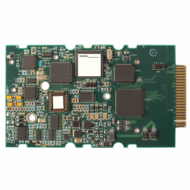
HDI (High-Density Interconnect) is the main difference between PCB design and manufacturing compared to conventional PCBs in they are more circuitry dense and hence the technological sophistication is very high These HDI offer smaller circuited line widths, smaller and finer vias, and the functionality of higher connection pad density, which are of high-miniaturized versions compared to the older ones. Its results are microvias, sequential builds, and laser-drilled PCBs, which are faulty, metres long but have the desired of producing superior electrical characteristics, performance, and miniaturization of devices.
Nine different general dielectric materials are used in HDI substrates.
Here are nine more components of different general dielectric materials commonly used in HDI (High-Density Interconnect) substrates:
FR-4: The most frequently used material in PCBs is the well-known polycarbonate, which has been used for a long time due to its good conduction characteristics as well as being heat-resistant and economical.
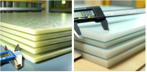
Polyimide: Offering superior thermal stability and engendering extraordinary flexibility, this material can be adopted in high-temperature applications and flexible high-density interconnect (HDI) circuits.
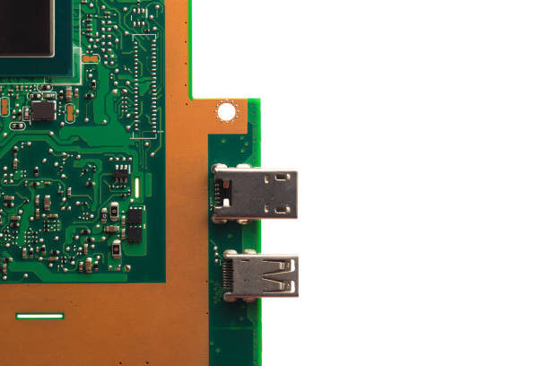
PTFE (Teflon): Estimated for its insanely low dielectric constant and loss factor, it is not wanting to disappoint during high-frequency transactions.
CEM-1, similar to FR-4 in function but more brittle and generally less expensive, is a good candidate for basic single- or double-sided PCBs.
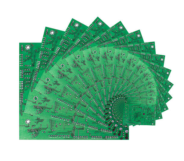
CEM-3: Like Fr-4, but with excellent RF performance and predominantly used in many-layer PCBs for high-density interconnection (HDI).
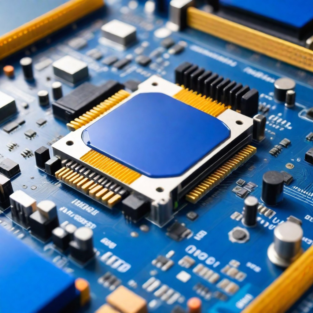
BT-Epoxy: Incorporating bismaleimide triazine and epoxy in a balanced way enables this material to give better thermal performance, making it good for rods of high speed or frequency.
Arlon: This kind is used for high-frequency applications and is being used for applications that require constant dielectric properties and high temperature resistance.
Rogers Material: A spectrum of high-efficiency substrates that have low dielectric loss, contributing to complex design structures and low power loss.
Liquid Crystal Polymer (LCP): A featured material composed of exceptional electrical characteristics and high chemical resistance that can make use of HDI PCBs (both flexible and rigid-flex) and high-frequency applications.
Overview of HDI PCB Board Design Processes
The design phases of HDI (High-Density Interconnect) boards are indeed highly detailed. Each of the steps is crucial to ensuring optimal performance and dependability of their final products. Here’s an overview of the key stages in the HDI PCB design process:
1. Specification and Planning
However, the process of design commencement for a product should be preceded by detailed electrical specifications, size constraints, proper component placement, and thermal management. Here, noting down the number of layers, the type of materials to be used, and the nature of connections and complexity are essential.
2. Schematic Design
Creators deem out their schematic design, which is a diagram that depicts the parts and their connections. This design step is essential in order to show all the electrical connections between the components as well as promote all the connections being handheld and mobile devices are made within the printed circuit board.
3. PCB Layout
Utilizing a unique software tool, the schematic layout is converted into a physical board layout. That is the time when PCB components are fixed and traces are organized in such a way that interconnections are made based on the schematic. In HDI PCBs, the via formation is related to the integration of microvias, blind vias, and buried vias , perhaps under the constraint of fine line technology to increase the density of interconnections in a smaller area.
4. Layer Stacking and Via Implementation
The layering would be structured in such a manner to maximize both electrical and structural integrity (the arrangement of the multiple PCB layers that is optimized for electrical performance and physical stability). There is generally a need stacked vias for sequential lamination process —the stacking up of one layer at a time and drilling—to enable more printed circuit board types (PCBs) with high miss stability. Vias are a more common connect option when you need to connect layers, improve their performance, and reduce the required space.
5. Signal Integrity Analysis
Since there is a higher density of connections, the process of HDI PCB signal integrity should be conducted with pre-studying. Simulating software is applied by designers to look at the rates in the high-speed signals and optimize their performance. Crosstalk, impedance mismatches, and signal attenuation are looked at by the software.
6. Thermal Management
The thermal significance study aims to detect the heat generated by the components correctly in order to dissipate it enough. Appropriate thermal protection is imperative in HDI PCBs if we want to avoid overheating and also maintain reliability.
7. Prototyping
In the process, the design should be awarded to get a sample to ensure that the circuit board works. The process incorporates the addressing of challenges at the pilot stage of production so that no errors creep into the exact model to be mass produced.
8. Production Preparation
At the end, development diagrams are created ready for manufacture, and it involves making Gerber files as well as any documentation needed for the PCB fabrication house. Particular instructions for this material, layer arrangement, via filling, and other HDI-detailed members have been involved.
9. Quality Assurance and Testing
Once done, HDI PCBs will go through a lot of testing to ensure they perform all functions as required and meet their exact specifications. This involves the likes of electrical tests, thermal tests, and visual inspection to find out any problems or failures in the structural integrity of the electrical appliance.
Trends in HDI PCB Design
Here are some concise trends in HDI PCB design:
- Miniaturization: The escalating integrated circuits’ capacity to pack the same volume of information in a smaller area and thus reduce the overall size and weight of the devices.
- Advanced Materials: Implementation of material systems with upgraded electricity conductivity and thermal properties to enhance operation.
- Microvias Technology: Spread the microvias that save a lot of space and improve the performance of the electricity.
- 3D Integration: On-boarding items can either be situated between the layers or on PCBs in order to occupy less space and improve signal integrity.
- Flexibility: Increased customer interest in HDI PCBs for use in smartwatches and other flexible devices. We will write a custom essay sample on Instruction: Humanize the given sentence. specifically for you for only
- Sustainability is an approach that focuses on environmentally conscious materials and technology.
- AI and Automation: Widespread adoption, digital and smart manufacturing processes with AI, and automation for optimization and efficiency.
- Improved Thermal Management: Heat dissipation technologies utilizing more advanced methods are being achieved in order to overcome the challenges of increased power density.
- Increased Speed and Frequency: The blocks of the design are tailored for higher signal speeds and frequencies, but, obviously, the signal impedance control and integrity management have to be present.
Design Your Feature Size to Satisfy HDI DFM Requirements
Developing your PCB for HDI device satisfaction with DFM (Design for Manufacturability) specifications involves making the right decisions across a range of key areas to ensure the reliable production of your board and reliable interconnect solution. Here’s a brief guide:
- Understand the Manufacturer’s Capabilities: These constraints should be considered, such as the trace width, via size, and the surface finish.
- Minimize Feature Sizes: Choose the minimum feature size that your fabrication path could accommodate competently and stably to get the higher density.
- Opt for Microvias: Substitute microvias for through-holes wherever possible so as to reduce material resources and decrease several layers.
- Control Trace and Space:Maintain the trace width and spacing for which the minimum is indicated so as to prevent shorts and secure signal integrity.
- Manage Aspect Ratio:Maintain the geometrical features of the via (depth to diameter) to ensure proper plating and the formation of a proper connection.
- Utilize Appropriate Pad Sizes: Design pads of this size to deal with soldering and assembly tolerance variations, especially in connection points like BGA.
- Employ Redundant Vias: Employ repeated vias through the crucial connection areas in order to enhance reliability in the event of their failure.
- Choose the Right Materials: Attention to the choice of materials in relation to thermal demand and the operational abilities of the design is essential.
- Verify with Simulation Tools: Leverage testing simulation of thermal, electronic, and mechanical processes to avoid last-stage defects and quality issues.
- Iterative Prototyping and Testing: Try creating a prototype and testing it many times so that the PCB doesn’t vary from the initial design specifications and performs better when used.
- Document Everything: Produce an unambiguous and comprehensive instruction manual for the manufacturing partner; every DFM element will be illustrated in the document to avoid mistakes and misinterpretation.
Benefits of HDI-Printed Circuit Boards

High-Density Interconnect (HDI) boards possess quite a few benefits compared with conventional PCBs, especially due to the fact that miniaturization of the electronics keeps happening with the need for increased performance. Here are the key benefits:
- Increased Density: In HDI PCB fabrication, less area is required to accommodate more complex features, which is ideal for miniaturized devices nowadays.
- Enhanced Electrical Performance: The faster signal transmission and good signal integrity that have become realities in HDI PCBs with shorter paths result from that.
- Improved Reliability: Microvia and advanced materials that are connected to HDI PCBs contribute to prolonging their sturdiness.
- Greater Design Efficiency: The HDI technology offers an alternative design to the PCB that eliminates the complex routing through the holes and increases production efficiency.
- Reduced Weight and Size: Along with being low and lighter in weight, these PCBs give us the best option for wearable and portable devices.
- Higher Component Density: So that the components of HDI board can keep the final circuit able, high-density is very ideal.
- Better Thermal Management: PCBs with good designs are capable of HDI, so better thermal conduction is ensured.
- Cost-Effective Production: Since HDI PCBs are made in high volumes, they are cheaper this way because they are made with fewer materials and processing steps.
- Faster Time-to-Market: The much faster design process of HDI PCBs is also another advantage since it can promote quick manufacture and delivery.
- Suitability for Advanced Technologies: Unlike many PCBs, HDI PCBs conform to the most recent tech advances and solutions.
Common Usage of High-Density Interconnect Printed Circuit Boards
HDI-printed circuit boards are widely used in applications implying both minimal space and weight as well as higher performance levels Here are some common uses especially to the advanced electronic medical devices:
- Smartphones and Tablets: HDI PCBs are the basic requirement for the development of thin and compact PCB patterns in the latest devices.
- Computers and Servers: Human-IC’s are the most important and essential type of PCBs for a smartwatch and a fitness tracker in small form factors.
- Wearable Technology: Medical portable devices applied in practice means HDI PCBs are used by them for being good-quality and small-size.
- Medical Devices: Medical portable devices applied in practice mean HDI PCBs are used by them for being good-quality and small-size.
- Automotive Electronics: HDI technology underpins the use of electronic devices in modern automobiles, which includes safety systems, among other simple aspects of entertainment.
- Aerospace and Defense: The stability of HDI PCBs heat and current made them suitable for the harsh environments of aerospace and military.
- Internet of Things (IoT): The idea IoT devices need density-printed circuit boards that come with both compact electronics and connectivity features, which is what makes HDI PCBs ideal.
- Telecommunications: They help in setting up the up-to-date communication infrastructure, like routers and switches, which offer improved signal integrity.
- Industrial Equipment: Besides designing HDI PCBs, one of the most influential points is the decrease of surfaces in the area of sensors and control systems.
- Consumer Electronics: In addition to phones, HDI-PCBs can be found in cameras, game consoles, or any other type of compact device.
What makes HDI boards different from the standard boards?
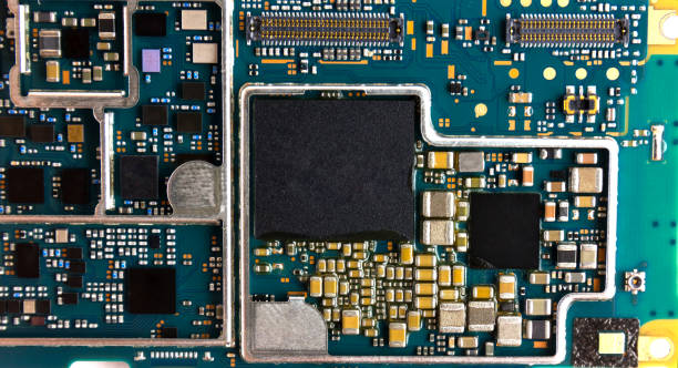
In a way, HDI (High-Density Interconnect) boards vary from a simple printed circuit board (PCB), where they excel in some features that are useful in the development of complex, compact designs. Here are the main differences:
- Via Technology:
- HDI Boards: Microvias come with a very short diameter, usually even less than 0.006 inches. Such types vary in different forms (they either connect an outer layer to an interior with only one connection or use only the inner layers with several connections made on top of each other or staggered for more space).
- Standard Boards: Normally used via holes with threading through the board from top to bottom layer, which require much more space and place a limit on the overall density of the design.
- Trace and Space:
- HDI Boards: The LSI chips feature much narrower lines and spaces (the cracks between the copper elements) than before, favoring more trenches per unit area.
- Standard Boards: Unlike human intelligence, which differs in speed and accuracy for perception, machine intelligence always contains wider traces and spaces; therefore, a board can only fit in a limited number of circuits.
- Layer Count and Configuration:
- HDI boards can use minimal space more efficiently with the use of microvias, making it possible to have more layers in a small print area.
- Standard boards typically feature two layers or fewer due to surface-mounted components with uncomplicated routing capabilities. Each through-hole via consumes more space due to its location; thus, adding an extra layer would require making the board a bit larger.
- Material and build quality:
- HDI Boards: Quite often, they use materials like print cloth in the spacing and embroidery to provide contrast. This involves the application of high-performance resins and glass styles that ensure better sustainability and electrical properties in RPA works.
- Standard Boards: The base material selection, other than conventional materials like standard FR-4, which are cheaper and perform below HDI materials, should be the primary aspect to be considered.
- Cost Implications:
- HDI Boards: In general, they are more expensive than conventional boards because of the highly sophisticated tools and materials required for production. Hence, they are more effective, but on the other hand, they go unnoticed in many fields of electronic technological applications.
- Standard boards are less expensive to generate and can be applied in niche channels and applications with low complexity and specificity.
- Design and Manufacturing Complexity:
- HDI Boards: The precision with which the microfluidic channels are designed and manufactured, encompassing laser etching or laser drill technology and advanced imaging processes, will be increased to allow the fabrication of the more finer features.
- Standard Boards: Maybe they can be manufactured using the traditional PCB manufacturing processes, which are less complicated and, consequently, more widely established.
Due to their unique features, HDI boards are widely sought after for advanced electronic technologies mobile devices that need to deal with high-speed performance, reliability, and size minimization. For instance, smart cell phones, tablets, medical devices, aerospace, and precision electronics are fields that extensively use HDI boards.
There are three types of stackups for boards they will assemble with hdi pcbs packages
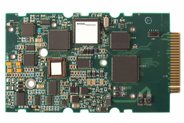
Assembly of HDI (high-density interconnect) PCBs is a process that requires careful consideration of the choice of stackup (the way in which the layers of the PCB are arranged), since the choice would directly affect the reliability of the board as well as its manufacturability. Here are three common types of stackups used in HDI PCBs:
Standard HDI Stackup
- Description: In a traditional HDI printed circuit board or hdi pcb stack ups process, you can expect one or more layers of HDI to be applied on the top and bottom DICF. This metrology features at least one layer of microvia sequence consisting of either blind and buried vias. The microvias are useful to have the outer layers connected to the adjacent inner layers. This hybrid interconnection structure is implemented by stacking or staggering the via’s.
- Advantages: This, in turn, makes it an affordable and feasible alternative to typical HDI outcomes in the production of relatively simple devices. It achieves better packing density than multilayer PCBs and similar high performance without incorporating the complexity and cost of advanced interconnect or via levels.
- Common Uses: These fields, as well as consumer electronics, automotive applications, and others, require various degrees of miniaturization and performance increment as an integral part of their operations.
2. Sequential Lamination Stackup
- Description: With the sequential lamination method, a number of lamination cycles are conducted, resulting in more laminated layers on the board. Hence, during this execution, burry vias and microvia structures of different levels can be embedded, such as stacked ones connecting various sites of the product. During each lamination cycle, more and more strands are formed until the full board structure is eventually created.
- Advantages: It provides a high circuit density and the possibility of making various designs with interdigital links in more than one layer. This topology serves SDSM (standard-defined multilayer), which is a circuit that has many connection points inside different layers on the printed circuit board.
- Common Uses: High-performance computing, telecommunications, military, and aerospace electronics are among the applications where reliability and density are of primary significance.
3. Every Layer Interconnect (ELIC) Stackup
- Description: ELIC is the industry-leading full-blown HDI system, with each PCB layer organized via micro-vias. This design covers the more complicated connections on the surface and is therefore one of the densest and most complicated HDI-PCBs.
- Advantages: When compared to the classical way of routing density and placement, which reduces the power of the board to the lowest possible value of the components, ELC provides maximum flexibility to design a board in such a manner that the maximum number of components can be placed and the interconnect paths are the shortest. Thus, low-loss signal transmission is ensured without compromising the quality of the transmitted signal.
- Common Uses: For delivering advanced consumer electronics types like smartphones and tablets that have very limited space and high-speed signal integrity segments that are significant.
Underlying this stackup is the choice of individual building blocks depending on the design objectives towards excellence, space, cost, and the constraints imposed by fabrication realization.
Conclusion
Control of advanced electronic technology is one of the key goals for designing HDI PCBs [HDI (high-density interconnect) PCBs]. Thus, only by understanding and applying new approaches and knowing what’s trending here and now would designers make up smarter, smaller, and much better grain machines. The further the technology develops, the more advanced and multi-faceted HDI (high-density interconnect) PCBs become, which current trends reveal as an extremely fascinating area with incredible potential in electronics.

