In the electronic industry, printed circuit boards (PCBs) play hidden characters and accomplish the achievement of numerous devices we depend on, such as mobile phones, computers, and televisions. However, it is interesting to know that while these appear to be unassuming containers, behind their deceptive façade there is a whole lot of complexity involved, in which even the simplest details like thickness can dramatically affect the way they perform. This blog post exposes you to the ongoing discussion of PCB thickness through analyzing how the optimized features of electronic devices can be improved by understanding standard thicknesses.
The Foundation of Electronics: PCB Basics

To get started on this topic of density, here are a few things that I would like to first understand. standard PCB copper thickness take on the exact role of the base in electronics when elements are connected and work together. Usually constructed from layers of substrate materials like fiberglass or epoxy resin, a PBC accommodates the network of conductive pathways that form the circuit that directs the electric signal.
Thickness Matters: Why It’s Crucial
Despite the low profile that the PCB thickness might have, it is, in fact, crucial for the successful mechanical stability, signal integrity, and reliability of the board while coping with the associated heat. Here’s why it matters:
- Mechanical Stability: A thinner PCB provides great rigidity, so it acts as good insurance against bending and warping during assembly and operations. It is a very essential feature in devices such as those that are used under the influence of vibration or mechanical impacts.
- Signal Integrity: The degree to which a PCB board influences signal transmission and impedance matching is highly dependent on its thickness. For example, one might encounter signal integrity problems, like reflections and amplifications, that may fail or work with low speeds and performance when the thickness is not in compliance with the design requirements.
- Thermal Management: While dealing with heat dissipation, electronic machines need to be followed scrupulously. Thick printed circuit boards have the attribute of providing multiple functions to electrical components, such as maintaining better thermal conductivity and heat dissipation, thus preventing overheating and preserving the component’s life.
What is standard PCB thickness?
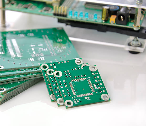
The normalized PCB width of about 1.6 mm is employed in so many applications, especially gaming or entertainment devices.
PCB Thickness and Manufacturing Process

PCB thickness is not just another dimension that interferes with print circuit board manufacturing; it affects different things, such as material selection and fabrication technique. Here’s how PCB thickness interacts with the manufacturing process:
- Material Selection: The selection of PCB material correlates with the required thickness. With the substrate materials FR-4, flexible substrate, or metal via, a range of different thicknesses can be met. The materials to be used by manufacturers are carefully chosen as per the mechanical property they are intended to possess, the rate of thermal conductivity, and the dielectric characteristic, which are all related to their thickness.
- Panelization and Handling: PCB’s are often produced in hard assemblies consisting of many individual boards. It is the PCB thickness that is crucial, as it determines the way these panels are made, assembled, and dispatched by the manufacturing process. It may require some procedures for the PCB core thickness to be changed to fit the actual parameter adjusted to the outside panel.
- Drilling and Plating: Along the PCB production line, vias are drilled to provide via holes for on-board components or to enable the interconnections between the layers of the board. The bespoke thickness of the PCB influences key principles like working speed, feed rate, and tool selection. Thicker PCBs might need derailing devices for openings, which are run on more robust equipment with various precise processes to comply with the exact hole dimensions.
- Copper Plating: Copper is electroplated onto the surface of the Patternal Broadcast Computer (PCB) to form a network of connecting points and pads. The rods of copper thickening influence the plating process, for instance, parameters such as plating times, current density, and solution composition. The plating of thicker boards PCB manufacturing would take longer than the plating of thinner PCBs in order to achieve the required copper thickness.
- Etching: Then, the extra copper weight PCB receives another etching treatment for its destruction. The etching parameters, like the etch concentration, temperature, and intensity of agitation, determine the degree of the PCB trace thickness derivation. PCBs of a greater thickness are often triggered in order to secure the completion of the etching process in the specified areas.
- Lamination and Pressing: Multilayer PCBs are made from multiple layers of substrate thickness materials and copper foils, which are bonded together with glue to create thin, insulated conductor sheets. Each layer’s thickness accordingly sums up to the final product’s thickness. The higher thickness of PCB can be realized by changing the lamination pressure (temperature), which is necessary for strong adhesion between layers.
- Surface Finish: The final PCB plating may therefore be different if the thickness of the various layers is altered. More thorough PCBs might require solder surfaces with greater solderability to secure a soldering with good wetting and adhesion in the presence of thermal masses with large dimensions or with copper being exposed.
Factors Influencing PCB copper Thickness
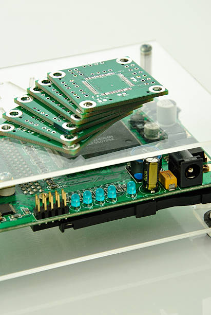
Several factors influence the choice of copper thickness in a PCB design:
- Current Carrying Capacity: The thickness of copper traces should be able to carry the peak current without overheating or losing the voltage when the current flows.
- Impedance Control: The thickness of copper foil influences the impedance of signal tracks. Achieving constancy of impedance is very necessary because damage to signal integrity reaching a higher frequency is caused by the application of high-speed digital, or RF.
- Heat Dissipation: The bigger copper layers have the capability to conduct the heat better, which in turn causes heat sinks near the elements to operate more efficiently.
- Mechanical Strength: processing Thicker copper layers result in higher mechanical strength, lowering the possibility of stray physical damage during the production chain.
- Manufacturing Capabilities: With the highly efficient copper thickness that the manufacturer can provide and process, the making of the product is easy and cost-efficient.
- Cost Considerations: The more copper foil layers or a single thicker pcb layer itself might compel the suppliers to include more materials or additional manufacturing procedures, which will eventually contribute to the higher cost of PCB production.
- Space Constraint’s small designs or multilayer PCB boards, there may be some limitations in terms of copper layer capacities, hence influencing the preferences for a given moderate-thickness profile.
Importance of PCB standard Thickness
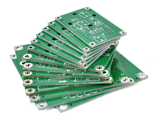
The standard thickness of a PCB is crucial for several reasons, including:
- Manufacturability: The primary thicknesses are commonly accepted by the fabrication process of PCBs, ensuring factory production and guaranteeing no obstacles.
- Compatibility: Standard-thickness PCBs are universally used in the industry, and they can be connected to other components, connectors, and enclosures as they are open to adapting the widely used parts.
- Interchangeability: Due to their standard thickness and interchangeability, PCBs with standard thickness can readily replace boards inside a product or across products. Sharing the same capacity helps in the simplification of maintenance and servicing.
- Signal Integrity: The PCB thickness refers of regular case typically comply with industry standard parameters for signal signal integrity, making it a problem-free product with regard to issues like impedance mismatching, signal degradation, etc.
- Thermal Management: The medium PCBs use bronze thermal properties, and they ensure good mechanical stability. It gives you the necessary rigidity to hold the parts firmly but also provides an avenue for heat dispersion.
- Cost-Effectiveness: Like the general PCBs, they become the subject of appropriate volume discounts as manufacturers tend to use the standardized ones more commonly. However, the custom thicknesses remain more preferable if cost-effectiveness is not the goal.
- Reliability: Moderately thick PCBs, due to their broad application and years of verification, provide a reliability and security level that may not be present in non-standard thicknesses. Hence, factoring in the reliability quotient, standard-thickness PCBs may be preferred.
PCB thickness specifications range in accordance with multiple factors like application, industry standards, and the limitations of actual production. However, some common thickness options include:
- Standard Thickness (1.6mm): The 1.6mm size is the standard PCB thickness employed in consumer electronics and most general applications, whereas the half-ounce thickness is usually the default thickness for digital power supplies and low-frequency networks.
- Thin PCBs (<1.6mm): Thin PCBs become components used in form-factor-critical products such as smartphones, wearables, and Internet of Things devices. They accomplish the same objective, though with a reduced weight and size but without the reduced performance parameter.
- Thick PCBs (>1.6mm): Industrial and high-power applications that demand more (thicker) PCBs in order to withstand higher voltages and currents are common. Ray boards offer improved mechanical and heat transfer performance.
What are the types of standard PCB thicknesses?
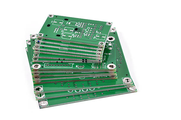
Standard PCB thicknesses can vary depending on industry practices, but some common options include:
1.6mm: This is the most conventional PCB thickness used for applications where a higher height is desired. This is for circuit board assembly (PCBA), and you will find them in most consumer electronics, industrial applications, and general-purpose prints.
1.0mm: PCBs fabricated of 1.6mm thickness are usually used where the size of the board needs to be minimized, for example, in portable devices, wearable equipment, and IoT devices.
0.8mm: As compared to the 1.0mm design, 0.8mm PCBs are vital in attaining miniaturization, where the ‘thinner the better’ design concept is adhered to, which is vital in ultra-compact electronic devices.
2.0mm and above: 2.0mm or above, which are more widespread, allow for the bearing of greater mechanical strength, increased endurance, and thermal management. This criticality is for multiple power electronics applications, industrial equipment, and automotive.
Here are a few examples of the common PCBs; the entire range may vary depending on the manufacturing company and their respective industry standards. The final thickness of the PCB determines the application needs, the mechanical limits, and the thermal and manufacturing impediments.
Tailoring pcb Thickness to Your Needs
The selection of the right PCB thickness is the result of a comprehensive consideration of a wide range of parameters that analyse the requirements of your project, environmental conditions, and budget limits. Maintaining contact with knowledgeable PCB designers and producers can give you an overview of the efficacy of your purpose. This is why you are able to achieve the aims and objectives you are after.
Calculating Your PCB Thickness and Layer Arrangement
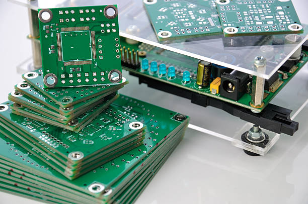
The mechanical needs, the electrical performance, and the constraints on manufacturing are included in the process of calculating the PCB thickness and the layer arrangement in the context of the particular objective. Here’s a step-by-step guide:
1. Determine mechanical requirements:
- Space Constraints: Indicate the minimal or maximum clearance that would limit the enclosure and the thickness limitations, if any.
- Mechanical Stability: Evaluate the necessity of flexibility to accomplish objectives and withstand environmental factors such as vibration or heat expansion.
2. Evaluate Electrical Performance:
- Signal Integrity: Mark out impedance levels for high-speed signal traces. For thicker copper or wider traces, one may be required to employ more and wider copper layers or traces, respectively, to realize the impedance of choice.
- Power Distribution: Compute the one-way power carrying values, trace, and planes. Thicker copper layers have greater superiority for the reduction of resistance and heat issues.
3. Consider Manufacturing Constraints:
- Available Materials: Be sure to select the PCB thickness variants from the list of available options by PCB material processors. Such standard thicknesses can range from 0.8mm, 1.0mm, 1.6mm, and 2.0mm, and custom lengths are available, but at higher prices.
- Fabrication Processes: Engage PCB manufacturers in order to understand their maximum number of board layers and board thickness. Some operations may be limited to quantities ranging from 0.32 to 0.65 mm.
4. Select Layer Arrangement:
- Single-Sided vs. Double-Sided vs. MultilayerDetermine whether a single-sided, double-sided or multilayer is required, according to the density of components, complexity of signals and routeing.
- Layer Stackup Design: Define sheet layers (such as signal, power, and ground) and their number and organization in order to reach the electrical performance and signaling quality that you want to have. Check impedance control, thermal management, and the shielding effect against EMI/RFI as well.
5. Perform calculations and simulations:
- Impedance Calculations: Consider impedance calculators or simulators to figure out sequence widths, clearances between traces, or multi-layer stack configurations to reach target impedance values.
- Thermal Analysis: Thermal simulations in this regard must be conducted in order to understand the heat dissipation capabilities and the selected thickness and layer arrangement to be able to manage heat loads.
6. Iterate and validate:
- Prototype Testing: Construct a perfect PCB in accordance with calculated and appreciated thicknesses and the sequence of layers. Perform tests to check for mechanical integrity, electrical functioning, and the capability of producing this item.
- Feedback and Optimization: Get feedback from prototypes, test, iterate, and modify the design when we realize there is an issue or an improvement that needs to be implemented.
Consideration of factors such as PGS, the extent of the thermal cycling effect, electrical requirements, and manufacturing practices is key to making your design meet the mechanical, electrical, and manufacturing needs of the application. Another crucial factor in this matter is working closely with a team of skilled PCB designers and associate makers, which can help a lot in the whole process of designing.
Conclusion
In the tiny world of electronics, you can see firsthand that even little things like the PCB thickness can bring a big change in performance and reliability. Engineers and designers will be able to fine-tune the performance of electronic equipment exponentially by comprehending the factors related to the standard PCB thickness and their influence on the strength of mechanical support, signal integrity, and thermal balance.
The PCB demystification process highlights that beyond the hood, there is more to the PCB than enhances functionality and performance. With the knack of this comprehension on hand, it will be possible for designers to glide through the complexities of PCB design with full confidence and assurance that they will attain the required supremacy in quality and dependability.

