It is copper thickness that makes printed circuit boards custom-designed and purposeful, as knowledge of the effect of thickness would result in great performance and reliability of the working electronics. This blog quite investigates the importance of the PCB copper thickness equal to 1oz and its applications with the PCB performance as a consequence.
What is 1 oz. Copper Thickness?
In making PCBs, copper weighs is measured in ounces per square foot. By “1 oz copper thickness,” we indicate the copper foil mass relatively uniformly catered over a square meter area as weighing one ounce. Hence, we get a figure of around 1.37 mils, which stands at 34.79 microns. Taken literally, it may appear to be very thin, and yet nothing can prevent it from being used in a number of different cases.
Weights measured in oz/ft2
The copper thickness is usually measured in ounces per square foot (oz/ft2), and the copper film is the standard setting quoted for a printed circuit board. This roughness is gravity, which defines the state of disarray or organized structure. Here’s how it works and why it’s used:
Copper Weight (oz/ft2)
- 0.5 oz
- 1 oz
- 2 oz
- 3 oz
- 4 oz
Thickness (mils)
- 0.7 mils
- 1.4 mils
- 2.8 mils
- 4.2 mils
- 5.6 mils
Thickness (microns)
- 17.78 microns
- 35.56 microns
- 71.12 microns
- 106.68 microns
- 142.24 microns
Benefits of 1 oz. Copper thickness
1 oz. copper thickness in PCBs offers several key benefits:
- Enhanced Current Capacity: facilitates the handling of higher amperage, lowering the risk of overheating, and draws a more powerful current for delivery.
- Better Heat Dissipation: This rapidly dissipates heat, which can prevent component failure and, therefore, prolong the durability of the PCB.
- Increased Durability: Enhances both the small bending properties and wear resistance, which are strong advantages in heavy-duty applications.
- Improved Reliability: This is the primary cause of most connectivity problems; these need to be avoided at all costs in order to ensure reliable and faultless electronic work.
Applications of 1 oz. Copper PCBs
1 oz. copper PCBs are commonly used in several applications due to their enhanced durability and electrical performance.
- Automotive Systems: Reliable operation in control systems, safety features, infotainment, and more are provided by the above-mentioned solutions.
- Power Supplies: Adequately for medium-power handling needs.
- LED Lighting: Perfect for dissipating heat from LEDs and therefore optimal for both their efficiency and a prolonged lifespan.
- Consumer Electronics: Which is one of the important properties that contribute to the performance of devices such as computers and TVs as related to thermal and electrical behavior?
key to converting to a linear copper thickness is knowing the density of pure copper
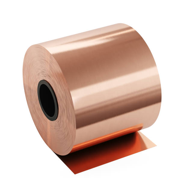
In fact, the secret to calculating copper bar measurement in terms of ounces per square foot (oz/ft2) to a linear unit, such as mils or microns, entails using the copper density. Here’s a brief explanation of how this conversion works:
Density of Copper
The copper has a density of about 8.96 grammes per cubic centimeter, or about 8960 kilograms per cubic meter (it equates to 8960 kilograms per cubic centimeter). Such is the reason that copper is the best choice of material for the transmission of power and heat.
Conversion Process
- Weight to Volume: First, convert the weight of copper (in troy ounces per square foot) to volume, then select the copper sheet of the desired thickness online, and finally input your order on the copper supply website. Density, or mass per unit volume, is what is represented by the formula density = mass / volume. The rearrangement yields an equation where volume = mass / density.
- Volume to Thickness: Thus, the volume per square foot can be found by multiplying the area of one square foot by the thickness value, usually expressed in mils, microns, or nano-pixels. Consequently, by dividing the volume (your rectangular prism, in which all dimensions are expressed in feet) by the area (one square foot), you will get the thickness.
Formula for thickness
Where:
- Copper is to the wt in oz/ft2.
- Copper density in oz/in³ is approximately 0.3214 oz/in³ when multiplied by copper’s density of 8.96 g/cm³ to obtain oz/in³ (1 cm³ = 0.06102 in³).
Key Properties of 1 oz. Copper
1 oz. of copper, commonly used in printed circuit boards (PCBs), possesses several key properties that make it highly suitable for a wide range of electronic applications:
- Thickness: This equates to 1.4 mils (approximately 35 microns in layman terms). This thickness of conductor has this unique form of flexibility and conducts high currents.
- Current Carrying Capacity: 1 oz of copper is, generally speaking, capable of at least 1.3 amps per mm of tracing thickness and may be even more suitable for carrying slew for moderate to high current loads.
- Heat Dissipation: Copper is a heat-conductive material, and a finished copper thickness of 1 oz coincides with transferring heat evenly around the electronic components, delivering the heat away from the components before they can overheat, causing failure of other components.
- Mechanical Strength:In fact, this 1-ounce copper layer might not be as strong as the thicker ones, but it is adequately tough for almost all the product operations and so is a suitable match for both consumer electronics and industrial areas.
- Cost-Effectiveness:1 oz. of copper is well-balanced between good performance and a low cost, making it suitable for use in PCB boards due to its ability to accommodate a wide array of applications. The thinner copper layer has, by itself, enough performance to run most standard platforms, and it does it with the benefit of lower printing costs.
- Versatility: Because of its moderate thickness and good conductivity, 1oz of copper-clad laminate may be employed in various applications ranging from routine electronic devices to any automotive and power electronics that are more complex.
PCB Copper Weight Designations (Copper Weights, Thickness (μm), Thickness (mils))
Weight designations in terms of copper features plates applied to PCBs mean the quantity of the copper and its thickness on the board. Here’s a table that outlines common copper weights along with their equivalent thicknesses in microns (μm) and mils:
Copper Weight (oz/ft2)
- 0.5 oz
- 1 oz
- 2 oz
- 3 oz
- 4 oz
Thickness (μm)
- 17.78
- 35.56
- 71.12
- 106.68
- 142.24
Thickness (mils)
- 0.7
- 1.4
- 2.8
- 4.2
- 5.6
Key Points:
- Copper Weight (oz/ft2): The given value is denominated in ounces per square foot at so many ounces per square foot of the copper-plated board.
- Thickness (μm) and (mils): The mechanical designers made replicas of these columns, which turned the weight of copper into thickness. A unit of measure that shows the dimension of one thousandth of an inch is one mil, and one thousandth of a millimeter is a micron. Calculations are based on the density of copper, with 1 oz/ft2 converting to approximately 35.56 micrometers or 1.4 mil of surface thickness.
Why Use 1 Ounce Copper?
Using 1 ounce of copper evenly in PCBs is beneficial for several reasons:
- Balanced Performance: It offers a fine balance of final thickness and wire to carry current, which means it is adaptable to multiple uses.
- Cost Efficiency: Provides a cheap option without compromising efficacy or quality.
- Heat Management: It usually effectively distributes heat, which amounts to maintaining the temperature of the electronic elements.
- Versatility: It is effective for both average and moderately elevated power circuits and is thus found in a broad rating area of numerous electronic devices.
Two-layer type in copper thickness
In a two-layer PCB, the thickness level of the heavier copper can be adjusted according to the individual characteristics of the aircraft, including power handling, thermal regulation, and mechanical strength. Here are some common copper thicknesses used in two-layer PCBs, such as inner layers and outer layers:
- 1 oz. copper: This is often the most popular standard of copper weight; other gauges (thicknesses) equate to roughly 35.6 microns and 1.4 mils (35.56 microns). It is the best choice for this purpose because it provides a good balance between cost, operation reliability, and good thermal management properties; therefore, it is suitable for numerous applications in consumer electronics and for lower power uses.
- 0.5 oz Copper: Thin at about 0.7 mils (17.78 microns), this is used where use requires lower power and finer widths of trace. This depends on the use. It is preferred in the case of a two-layer board, but it is sometimes chosen for weight savings and low-current applications.
- 2 oz. Copper: Thinner, at about two and eight mils (71.12 microns), this level of thickness supports greater current loads and more effective heat dissipation, which makes it ideal for power electronics and also automotive projects where efficiency and robustness are necessary.
Comparing 1 oz. to Other Copper Weights
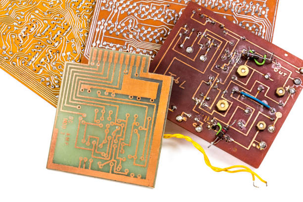
1 oz of copper is then compared with other weights of copper in electronic devices like PCBs, from the perspective of electrical performance, thermal management, and mechanical properties of copper. Here’s a comparison of 1 oz of copper with other common weights like 0.5 oz, 2 oz, and higher:
0.5 oz Copper
- Thickness: It is about 0.7 mils. ?From the other side, this number equals 17,78 microns.
- Current Capacity: lower than 1 ω; it is useful for other types of experimental work that do not consume high current.
- Applications: It can accommodate low-power devices or when the traces will only be fine, such as when a finer width of conductive lines is required in high-density, lower-current consumer electronics.
1 oz. Copper
- Thickness: 1.4 mils is approximately 35.56 microns.
- Current Capacity: The reclaimed plastic can be widely used since it can withstand high seawater resistance.
- Applications: Generally used in consumer electronics and automotive electronics, it is associated with a range of ordinary applications, including applications where performance-cost balance is required.
2 oz. Copper
- Thickness: About 2.8 mils (an equivalent of 71.12 microns).
- Current Capacity: Higher than 1 oz; can easily deal with large currents; and has better heat dissipation features.
- Applications: Workable for power electronics, automotive parts, and everyday devices whose reliability is dependent on efficient power handling and heat dissipation.
Higher Weights (3 oz. and Above)
- Thickness: The tear strength is.001 (106.68 microns) for a 3 oz weight, incrementing as weight increases.
- Current Capacity: Extremely high; these ratings are only suitable for applications with norms and requirements with significantly higher power capabilities and thermal management capabilities.
- Applications: Used in industry, essential in large power converters, and one does not dare to design applications for certain extreme conditions, like in aerospace and military electronics.
When Higher Copper Weights Are Required
Higher copper concentrations, copper tracks that handle higher currents, enhance thermal management capabilities, and improve mechanical strength are needed in this scenario. Here are some common situations that necessitate the use of thicker copper layers:
- High Power Applications: The devices that manage very large power, such as motors, power supply units, and DC-AC power converters, require thicker copper to manage larger currents more effectively.
- Thermal Management Needs: In situations where a large amount of heat is generated by the electronic components, how much copper assists in the rapid and more efficient conveying of the heat away, which prevents overheating and the occurrence of reliability breakdowns on the device?
- Mechanical Durability: In the cases of PCBs that operate in circumstances where their elements are exposed to physical stresses, for instance, cars or industrial power plants, copper with a higher thickness will add to the structural stability of the board and render it more robust and sturdy.
- Longevity and Reliability: With applications where the life of the product is essential, as in aerospace and military, heavy weights like copper are used in order to guarantee that the cars will serve in the toughest conditions and continue long-term operation.
Choosing the Right Copper Thickness
While 1 oz. of copper offers many advantages, it’s crucial to consider your specific application requirements:
- Current Requirements: Carry out the power flow of every retraced path. Greater currents need to be distributed along the copper lines, which may lead to heating up the traces and even voltage drops.
- Thermal Management Needs: Resistance to heat is also one of copper’s attributes. As such, thicker cuppers are the best to tackle heat problems by transferring heat and keeping the device from getting too warm.
- Physical Environment: For the purpose of your PCB, think of the obvious physical stresses it might experience. The body of copper has to be able to provide extra strength and rigidity for additional coating.
Conclusion
The heavy copper voltage level is an embodiment of the strategic choice of applications that can effectively endure unprecedented power distributions, be able to control heat distribution, and have increased durability. The greatest advantage of this method is that it is strongly required for medium- and high-power electronics in automotive and industrial applications, which have significant current handling enhancement and heat dissipation as their major features. Besides, copper, with its designated structure allowing it to hold up against the rigors of harsh operating conditions, gives the parts the durability needed to meet their platform’s dynamic environment. Incorporating a heavy copper interface in your PCB design allows you to have an adequately robust product that performs under stress, hence a product that works longer with less downtime.

