The world of electronics is like a puzzle of complicated jigsaws, where successful PCB reverse engineering is a tool to solve it. This is done by opening the item and seeing how it functions, since usually there is no original construction instruction available. Producing printed circuit boards (PCBs) of different types with their laminated layers and electronic components is thus quickly becoming a target for reverse engineering. This practice does not only help to grasp the technical aspects of modern electronics but can also serve as a foundation for further undiscovered territory in terms of technology design and security analysis.
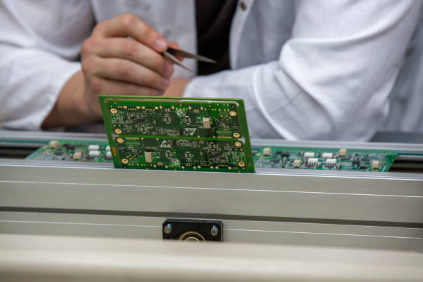
This guide goes deep into the intricacies of how to do PCB reverse engineering. It is not only practiced by enthusiasts and professionals but also by people who find it an art and a science.
What is PCB reverse engineering?
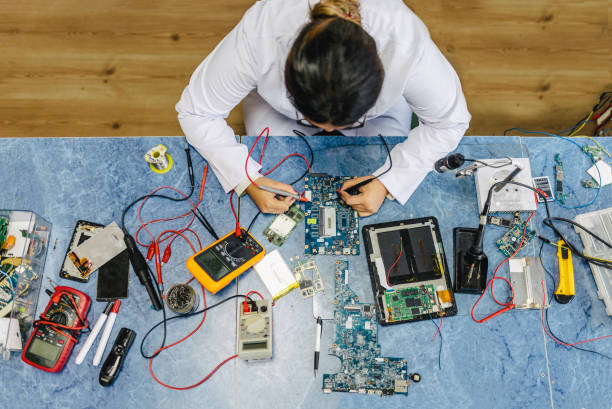
PCB reverse engineering is the method by which the last design data about a physical PCB, which includes schematics, bill of material (BOM), and layout information, is analyzed and extracted. This can be for purposes such as replicating the design of a PCB that is not available anymore, understanding how a competing product works, or verifying whether an idea patented by someone else has infringed on patents held by others.
What are the benefits of reverse engineering a PCB?
Reverse engineering a PCB offers several benefits:
- Documentation Recovery: Allows the rediscovery of non-current design documents.
- Enhanced Understanding: Allows for much more comprehensive information relating to the structures and operating principles of the PCB.
- Innovation: Enables the creation of novel solutions through the application of good practices and the introduction of improvements to designs.
- Competitive Analysis: Provides data analysis for competitor products that enables the evaluation of specifications and functionality to benchmark with competitors’ products.
- Security Evaluation: Contributes to locating shortcomings and amplifying the defense levels of electronic circuitry.
- Cost Reduction: The overall costs can be brought down through the replication of designs already in production.
- Legacy Support: This supports the remaining service life of obsolete systems, but the vendor is not capable of offering further upgrades to them.
- Educational Value: Provides an ideal learning opportunity for both students and people who deal with electronic stuff.
How does the PCB reverse engineering process work?

Printed circuit board design discovery begins with the reverse engineering process, which involves multiple steps to find out the board design and operating mechanism. Here’s a step-by-step guide to reverse engineering a PCB:
Step 1: Preparation
- Gather Tools: Ensure that you have access to all tools, i.e., a digital multimeter, an oscilloscope, soldering equipment, and possibly X-ray or CT scanning for multilayer or thicker boards.
- Documentation: Make as good records about the original board as possible through high-resolution photos from different views.
Step 2: Visual Inspection
- Examine the PCB, including its connections to each other. Take down or take note of any labels, color codes, and the apparent layout of traces and internal layers. Add
Step 3: Schematic Creation
- Trace Circuits: Apart from the multimeter, put it to work to trace the components firm connections. Thus, a schematic PCB concept is created.
- Circuit Mapping: Present design onto the circuit if the skills are at a high level, either manually or by using electronic design automation (EDA) reverse engineering pcbs or pcb reverse engineering software for easier and faster connection and component mapping.
Step 4: Component Identification
- List Components: Acknowledge and mark every item, for example, the resistors, capacitors, integrated circuits (ICs), etc., with their values and positions.
- Datasheets: Collect data sheets of all pinpointed parts to comprehend their particularations and operational modes.
Step 5: De-layering (for Multilayer PCBs)
- Physical or chemical de-layering: carefully removing the different layers to expose the inner circuits. This can be done organically or by harsh chemical methods; however, it mostly leads to the spoilage of the top soil.
- Non-destructive Methods: In other types of imaging, such as X-rays, we can conduct internal layer-by-layer observation without disassembling the PCB.
Step 6: Digital Imaging and Analysis
- High-Resolution Imaging: Scan the PCB closely with a scanner of high resolution to capture a high-quality image of each layer.
- Image Analysis: Apply the image processing algorithm to deconstruct and reconstruct the layers and trace routines.
Step 7: CAD Reconstruction
- Recreate Design: Utilizing the given image and schematics, create an authentic PCB design using CAD software equating the actual design.
- Adjustments and Optimization: Adapt the model according to the fabrication process or progress for a better product.
Step 8: Prototyping and Testing
- Prototype Manufacturing: Implement a PCB replication using a PCB manufacturing vendor.
- Functional Testing: Thoroughly test the prototype so as to confirm that it has all the functions and parameters equal to those of the original model. Re-arrange the design once the test shows the designs are suitable.
Step 9: Documentation
- Create Detailed Documentation: Accurately document every stage of the process and all the details of the design in the form of schematics, parts listings, CAD files, and testing findings. With this important document, there will be no difficulties or confusion when production starts.
Additional Tips:
- Legal Considerations: Be mindful of the legal matters that may come up while exploring reverse engineering, especially those related to intellectual property laws and patents.
- Skill Development: Practicing with PCB design tools, soldering, and circuit analysis gives a huge opportunity to gain the necessary skills for successful reverse engineering.
Why reverse engineer a PCB?
A PCB (Printed Circuit Board) may be reverse engineered to give out various advantages that could be transferred between and also sectors, for instance, the electronics and cybersecurity ones. Here are some key reasons why someone might choose to reverse engineer a PCB:
- Understanding Existing Designs: Reverse engineering gives the possibility to widen designer’s and engineers’ knowledge in this field when distressed by old systems or systems with incomplete documentation.
- Competitive Analysis: The technology policy of monitoring rivals’ items and comparing them is usually dispersed by companies. This study can manifest certain information, such as features, cost structures, and manufacturing techniques.
- Educational Purposes: For both learners of electronics and circuit design as well as professionals, unauthorized reverse-engineering real-world PCBs will provide the experience of a real item and will help the students to understand the electronics design principles more deeply.
- Enhancing or Customizing Products: Through better understanding the PCB function, engineers will be able to improve the product in terms of adding modified or enhanced functionality or introducing more features that make it more competitive, relevant, and needed in the market.
- Obsolescence Management: Identification of various components of an industry that may have become obsolete for use can then help in the reverse engineering process for the purpose of identifying their equivalent and substitute parts that can replace them without the need for a complete system redesign.
- Security Analysis: In cybersecurity, reverse engineering is used to find the weaknesses of hardware design or possible backdoor exploitation in a PCB. This is a major element of the task of providing security for cyber systems.
- Cost Reduction: Through this way of recreating, enterprises can replicate or manufacture the previous design more efficiently by minimizing the risks, for example, the costly R&D processes of establishing the same or similar technologies.
- Documentation Creation: As far as products that lack adequate documentation because of age, loss, or improper management, reverse engineering enables engineers to reconstruct an accurate manufacturing and documentation file, which is useful for maintaining an up-to-date code of compliance.
- Legal and IP Considerations: Additionally, reverse engineering can be utilized to detect potential violations of patents or to remain up-to-date on intellectual property laws; this, however, needs to be carried out with due legal guidance in order to avoid litigation.
- Recovery and Disaster Analysis: In situations where hardware damage leads to substantial operational discontinuity, reverse engineering the failed PCB can assist engineers in resolving the failure and mitigating future recurrences.
Tools and Technologies in pcb reverse engineering
The technology and tooling used in this process range from very specific to computer-aided. Here’s a breakdown of some of the most essential tools and technologies used in the process:
Multimeters
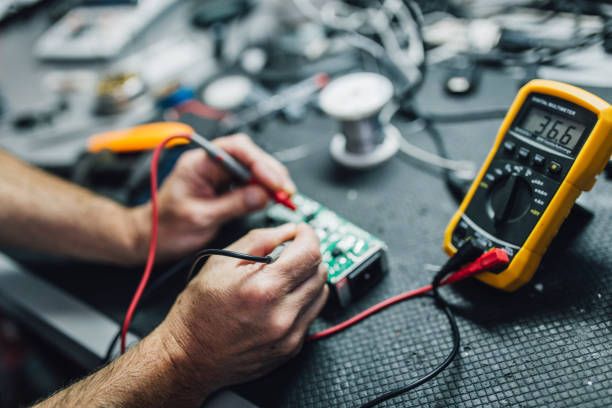
- Purpose: Electricians may rely on this for the identification and control of basic voltage, current, and resistance measurements.
- Use in Reverse Engineering: It helps reduce the chances of error at the component level, as well as helps in choosing the correct values of components.
2. Oscilloscopes
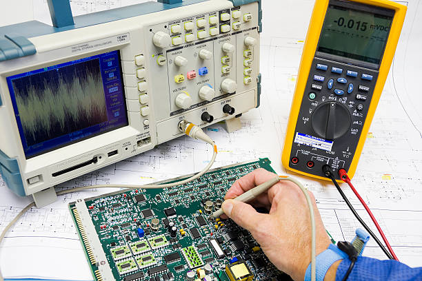
- Purpose: Harness voltage signals and visualize them through a waveform.
- Use in Reverse Engineering: Can be used to detect and measure the movement of electronic signals within the circuit.
3. Schematic Capture Software

- Purpose: Used to build the circuit diagram by drawing and naming the parts of the circuit.
- Use in Reverse Engineering: Enables the creation of a diagram showing the exact circuit arrangement and the wires going from one component to the other.
4. PCB Design Software (CAD)

- Purpose: They are utilized to produce and shape electronic PCBs.
- Use in Reverse Engineering: Some software produces PCB designs, which are analyzed so that the circuit can be modified and optimized.
5. X-ray Imaging
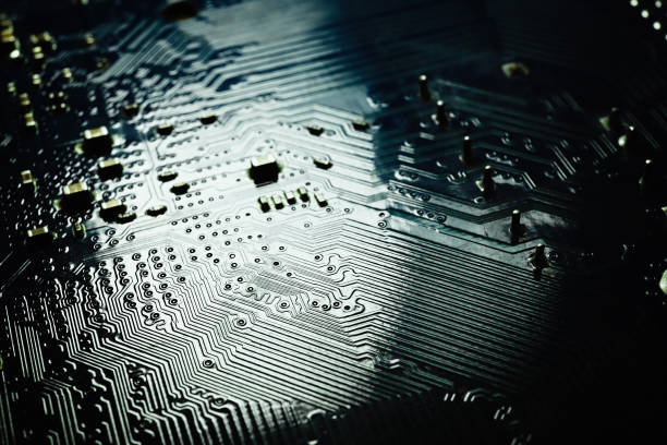
- Purpose: Provide a destricture-free option for looking at the different pcb layers of multiple-thickness PCBs.
- Use in Reverse Engineering: In addition, the multitude is also a crucial factor when it comes to the analysis of various layers, potentially without damaging the PCB.
6. Logic Analyzers
- Purpose: Placing and displaying digital signals to be able to distinguish digital circuits that are complex to debug.
- Use in Reverse Engineering: It is valuable in analyzing digital communication, and in some cases, it can be leveraged as a digital circuit verification tool during the design stage.
7. Signal Generators
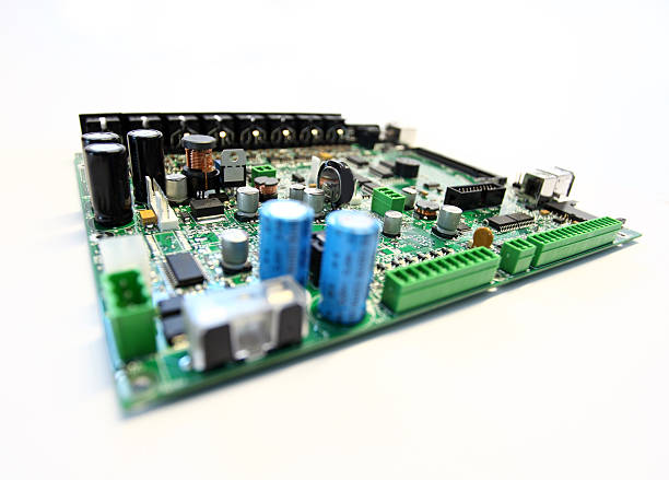
- Purpose: Replicate data-generated electrical types (sine, square, triangular, etc.).
- Use in Reverse Engineering: Sustained to operate logic circuits and measure response, it constitutes an important surface mount device for evaluating the functioning of a circuit in a way that is expected.
8. De-soldering and Re-soldering Equipment
- Purpose: To remove and replace obsolete components on the print circuit board.
- Use in Reverse Engineering: Core, which allows for part identification and breakdown by bringing out the individual obsolete components for internal investigation.
9. Microscopes and Inspection Equipment
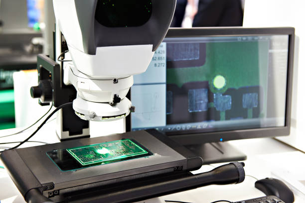
- Purpose: The larger the area, the smaller the object, or the trace, can be examined and analyzed in depth.
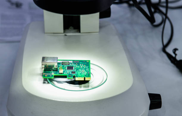
- Use in Reverse Engineering: It is critical to examine the solder joints, trace the integrity, and on densely populated PCB layouts, unopen all the components labels.
10. Layer Peeling Tools

- Purpose: Chemically or mechanically remove a multilayer PCB.
- Use in Reverse Engineering: Provides the chance of inspecting the interior structures; however, the method is destructive.
11. High-resolution Scanners
- Purpose: Model graphical images of printed circuit boards.
- Use in Reverse Engineering: Expand the digital creation of the PCB layout via highly detailed images of each template layer.
12. Software for Simulation and Testing
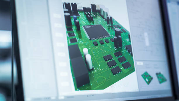
- Purpose: Simulate electronic devices circuitry to evaluate its behavior when altered by different conditions.
- Use in Reverse Engineering: Verifies the functionality of the circuit according to a created model using the simulation software and then progresses to the prototype stage.
13. 3D Scanners
- Purpose: Make a 3D prototype of the PCB.
- Use in Reverse Engineering: Aids in documenting the dimensional data of the circuits or models, which helps in clarifying mechanical movement and fits in the assembly.
Challenges in PCB Reverse Engineering
The rebuilding of the PCB (Printed Circuit Board) is a complex and hard job for the same reasons—technical, legal, and ethical factors. Here are some of the main challenges faced in PCB reverse engineering:
1. Complexity of Modern PCBs
- As the nature of modern PCBs transforms into multi-layer designs with very small and densely packed components and very complicated routes, it would be challenging to decipher and document them correctly. The newest techniques of HDI and microvia with additional precision levels simply won’t be solved without high-end equipment that can’t be just assumed.
2. Access to the Inner Layers
- For multilayer PCBs, the inner layers become invisible since the inside layers are not supposed to be seen. Hockey methods like X-rays may prove to be useful, but they are pretty costly and unsustainable. Another problem with physical deflux is the fact that harsh solvents always tear the boards to pieces, which may lead to traces or components being destroyed.
3. Identifying Unknown Components
- Labeling of components that are either unclear or custom-made typically applies to certain applications and causes a lot of difficulties when identifying such components. What is needed are either deep research or direct connections with producers (which may be impossible at some point in time or restricted), and sometimes there is no handle on them.
4. Accurate Schematic Recreation
- Developing consistent schematic records from obsolete boards in the presence of complexity in the circuits or modifications that were not initiated are aspects that can be very hard to grasp. It is a destructive process that entails mastering the basics of electrical circuitry, and that can be fairly tedious sometimes.
5. Software Limitations
- But there are software programs for PCB design and circuit simulation ready to use, though they could have some limitations in working with some file formats, or you could be stuck without the support of reverse engineering. It is important to check if the software programs are a true reflection of the PCB’s original physical aspect.
6. Intellectual Property and Legal Issues
- Reverse engineering may generate lots of problems with the law, maybe concerning copyright, patents, and trade secrets. However, avoiding legal hurdles by getting the right legal knowledge is very important while setting forth reverse-engineered PCB making, particularly if it is meant for commercial use.
7. Ethical Considerations
- Reverse-engineered products bring whole new ethical intricacies concerning why they are being devised and used. It is very crucial to reflect on the motive of this reverse engineering, whether it is undertaken to widen the intellectual understanding of a product or if it breaches the inventors’ intellectual ownership and profitability rights.
8. Skill and Resource Intensity
- It entails having high levels of expertise in many sub-fields, which can be in software, electronics, and sometimes even mechanical engineering. In this regard, the distribution of competent instruments and technologies and their cost can also represent a barrier, mainly for small organisations or individuals.
9. Testing and Validation
- Since exact replication of the present design without any changes is a must, a reverse-engineered PCB requires multiple iterations and validations in the end. There are stringent measures of control needed for documentation, components, and assembly so that no errors can occur.
10. Data Integrity and Management
- The data management challenge during the reverse engineering process, characterized by a number of different imaging, measurement, and test results, demands competent data management strategies so that data quality is enhanced and data access is facilitated.
What are the calculations using formulas in PCB reverse engineering?
Calculation and formulas are an integral part of PCB reverse engineering or destructive reverse engineering, helping in the understanding and reproduction of circuit functioning.
Description:
- Ohm’s Law binding principle, which is used to determine voltage (V), current (I), or resistance (R),. Verification on the component level can be done by one of these fundamental laws.
- Trace width is determined according to the actual current load and permissible temperature rise. It is necessary to realize this type of production to be able to protect circuits from physical damage.
- Capacitive Reactance The operational capacitive reactance at different frequencies that helps understand and analyze the behavior of the capacitors is calculated.
- Inductive Reactance With its reactance capacity, inductive reactance is being counted as a crucial analysis to do an inductors flow in the system
- The RC time constant is calculated to estimate the time constant of an RC circuit that is needed to forecast how fast the circuit reacts to voltage changes.
- Resonant Frequency (LC Circuit) It finds out the resonant frequency of an LC circuit, and this is what helps in circuits that operate at a particular frequency as designed.
- Power dissipation in resistors helps calculate the power that flows via resistors, which in turn helps ensure that the components will be operated within safe parameters.
- Voltage Divider Determination of an Output Voltage in a Voltage Divider Circuit is the Must Answer for Circuit Design with Definitive Voltage Requirements.
- Decibel gain/loss, an approximate result of the range of power across components, is used mostly in signal processing and analysis.
Applications of PCB Reverse Engineering
Reverse engineering a PCB (Printed Circuit Board) is an activity that comprises various stages that are connected in a way that provides a flow for different applications. Its flexibility is the other aspect that contributes to increased demand from various industries. Here are some key applications:
Legacy Systems Maintenance
- Application: When it comes to older systems where documentation is lost, an old diagram/design doesn’t exist, or even new parts are needed for the system’s components, reverse engineering the system represents an effective solution for maintenance and updates without a total redesign.
2. Competitive Analysis
- Application: Reverse engineering is particularly useful for companies in the sense that it involves the analysis of the products of competitors. This helps in comprehending the technologies employed, cost, and areas of benefit to the company itself.
3. Counterfeit Analysis
- Application: Consumer fraud in the electronics sector is generally due to counterfeit products, which the sector is able to avoid by comparing the products to original designs, thereby not only protecting brand integrity but also consumer safety.
4. Cost Reduction
- Application: The goal of the firm to achieve the optimal manufacturing process, which will lead to cost reduction and improved product performance, becomes possible through an understanding of the detailed manufacturing & functional aspects of a PCB.
5. Educational Purposes
- Application: Reverse engineering embodies both practical and educational functions, serving as a handy device for students, engineers, and designers to gain knowledge of the circuit design process, problem solving, and manufacturing.
6. Security Testing
- Application: In the industry of cybersecurity and defense, reverse engineering happens to find out the hardware flaws that may be used by hostile forces for their own harm. The software in this case serves the purpose of securing the hardware units.
7. Intellectual Property Cases
- Application: It can be applied to validate the claims of a patent or to decide on intellectual licensing disputes since the microscopic detail of the function of the device or its internal structure can be provided with this device.
8. Customization for Enhanced Functionality
- Application: Often, engineers would reverse engineer PCBs to enhance their function or modify existing electronics for new purposes. The goal, therefore, would be to increase their functionality as well as the lifecycle of electronic products.
9. Product Updates and Upgrades
- Application: For products that need updating or newly imposed regulations in operation, reverse engineering could be used as a method to design the latest PCBs or comply with current technologies or regulations.
10. Failure Analysis
- Application: The advantage of reverse engineering is that when e-products break down, this process helps to find the root cause of the failure and lets developers develop more resilient and reliable electronic systems.
Design Validation and Troubleshooting of pcb reverse engineering
Objective: This was to validate the reverse-engineered PCB by copying the original design with all label component specifications so the repeated one could be functional.
Steps Involved:
- Schematic Verification: Verify the validity of the schematic against the technical diagram by tracing the PCB to find out that all the connections and parts are in the correct position.
- Prototype Testing: Make a working model based on a blueprint that is drawn out from the analysis of the original product. This first version, in turn, undergo a procedure of testing that is far-reaching
- Functional Testing: Conduct functional testing and compare the outputs of your board to match the actual board to verify that each core functionality of the sample PCB works as planned.
- Environmental Testing Immerse the UAV in different climate conditions (temperature and humidity) to maintain overall stability and reliability in different working environments.
- Compliance Testing: Confirm the PCB image is up to current standards and legislative requirements, which may include electromagnetic compatibility (EMC) tests, safety standards, as well as other requirements.
Troubleshooting in PCB Reverse Engineering
Objective: To identify and amend defects of declining, failure, or performance in updated PCBs, we will use reverse-engineered PCBs.
Steps Involved:
- Error Identification: Use your instrumentation to determine which parts of the PCB are not performing as expected and take corrective measures for their improvement. With incorrect signal timing, unforeseen values, and frailties of components, failure of the system overall might be the result.
- Component Analysis: Completely carry out and try all pieces of the device; however, their failures and discrepancies should be part of the analysis. Isolation of these faults may require remeasurement of component values or replacement of components already determined to be faulty by the diagnosis tools. Test for issues as to crosstalk, noise, and signal drop-off. Utilize instruments that can monitor and measure waveforms simultaneously, such as an oscilloscope and logic analyzer, to guarantee signal integrity board-wide.
- Signal Integrity Analysis: On hot spots indicating that some components of the PCB are overloaded or distributed power is not performed properly, which are problems of faulty PCB designs, utilize thermal cameras.
- Thermal Imaging: On hot spots indicating that some components of the PCB are overloaded or distributed power is not performed properly, which are problems of faulty PCB designs, utilize thermal cameras.
- Iterative Testing: Use the top-down approach by attempting to make some changes at one time and working on them through trials. This type of method plays the role of isolating variables into pieces and ascertaining the effect of each one on the entire PCB performance.
- Documentation Update: Update documentation all the way along the troubleshooting process, showing all the changes and being a useful source of information when the next phase of maintenance or another version has to be done.
Tools Used in Validation and Troubleshooting
- Simulation Software: As it is about reliability and production testing of the complex, high-density PCBs,.
- Automated Test Equipment (ATE): As it is about reliability and production testing of the complex, high-density PCBs,.
- Specialized Testing Rigs: Flexible settings that emulate the location of real-life PCB operation.
Challenges and Limitations of PCB Reverse Engineering
PCB reverse engineering involves several challenges and limitations that can complicate the process:
- Complexity: Pre-modern PCB assemblies were generally composed of a limited number of components and single layers, in contrast to the densely packed multi-layer designs of micro-scale contemporary components.
- Access to Layers: Access to the interior of the multilayer PCB, without its damage, can sometimes turn out to be a difficult task, and mostly this is possible only with the help of specialized equipment like X-ray machines.
- Component Identification: Locating the sources of unmarked or individual parts could be a tiresome task and could be done via extensive research work or otherwise.
- Legal Issues: Interestingly, the issue of reverse engineering can result in lawsuits, primarily in connection with intellectual property laws and copyrighted works.
- Technical Expertise: For an effective PCB Schematic Design, high levels of technical information, such as experience and knowledge in the interpretation and reconstruction of intricate circuits, are of great value.
- Time and Cost: The process may take more time and can be costly due to the expertise of the workers and the complex equipment involved.
- Accuracy of Documentation: As the reverse-engineered product gets replicated, the original design gets enlarged unnecessarily.
- Ethical Concerns: Ethical factors need to be taken into account, in particular when copyrights are used while copying or compromising the property.
Additional Tips for pcb reverse engineering
- Legal Considerations: Remember that reverse engineering is a legal term; study it thoroughly and its relation to copyright and patents.
- Skill Development: Through a series of PCB design software, soldering, and circuit analysis, you will be able to deal with the reverse engineering process successfully.
Conclusion
PCB reverse engineering is a laborious and complex process with multiple aspects, which is always of great significance when it comes to getting the system to function, keeping it in working condition, and developing it further. Students approach this by disassembling the circuit boards, and by so doing, they acquire skills that are essential for circuit construction, failure detection, and legal. Implementation of design changes or improvements in existing PCBs circumvention of documentation is an irreplaceable aid, particularly in the context of keeping systems up-to-date and a security matter. On the other hand, the process involves technical issues, e.g., legal and ethical matters. The advancement of technology results in continuous improvement of the reverse engineering tools and techniques used in the field, making them more reliable and better insulated from the surrounding environment. Professionals in this field must be prepared to understand these advancements and address these issues, such as best practices and legal standards, which will help maximize the benefits of reverse engineering printed circuit boards.

